24
Catalog
I Introduction | |
II Prevention of PCB warping During Processing | 2.1 Prevent the Warping Due to Improper Inventory Mode |
2.2 Avoid Warping Caused by Improper Design and Processing | |
2.3 Eliminate Stress on Substrate | |
2.4 Baking Board | |
III Leveling Method of PCB warping | 3.1 Level Warping in time in the Production of PCB Boards |
3.2 Leveling Method of Finished PCB Warping | |
3.3 Hot-pressing Leveling Method with an Arc Mold | |
IV Conclusion | |
PCB Bowing and Twisting
I Introduction
People in the industry must be fairly aware of the influence of PCB warping. For example, it will hinder the installation of SMT electronic components, make the electronic components (including the manifold block) in poor contact with the solder joint of PCB board, or make it difficult to cut the foot when all the electronic components are mounted, and during the process of wave soldering, some parts of bonding pad on the substrate can not connect with the solder side because of the warping.
The main cause of the PCB warping is that the substrate (copper clad laminate laminate) is warped. Besides, during the processing of the PCB board, due to the influence of the thermal stress, chemical influence, and improper production process, will also lead to PCB warping.
Therefore, for PCB board manufacturers, the first is to prevent the PCB warping during processing; and for PCB board that has already warped, there should be a suitable and effective treatment method.
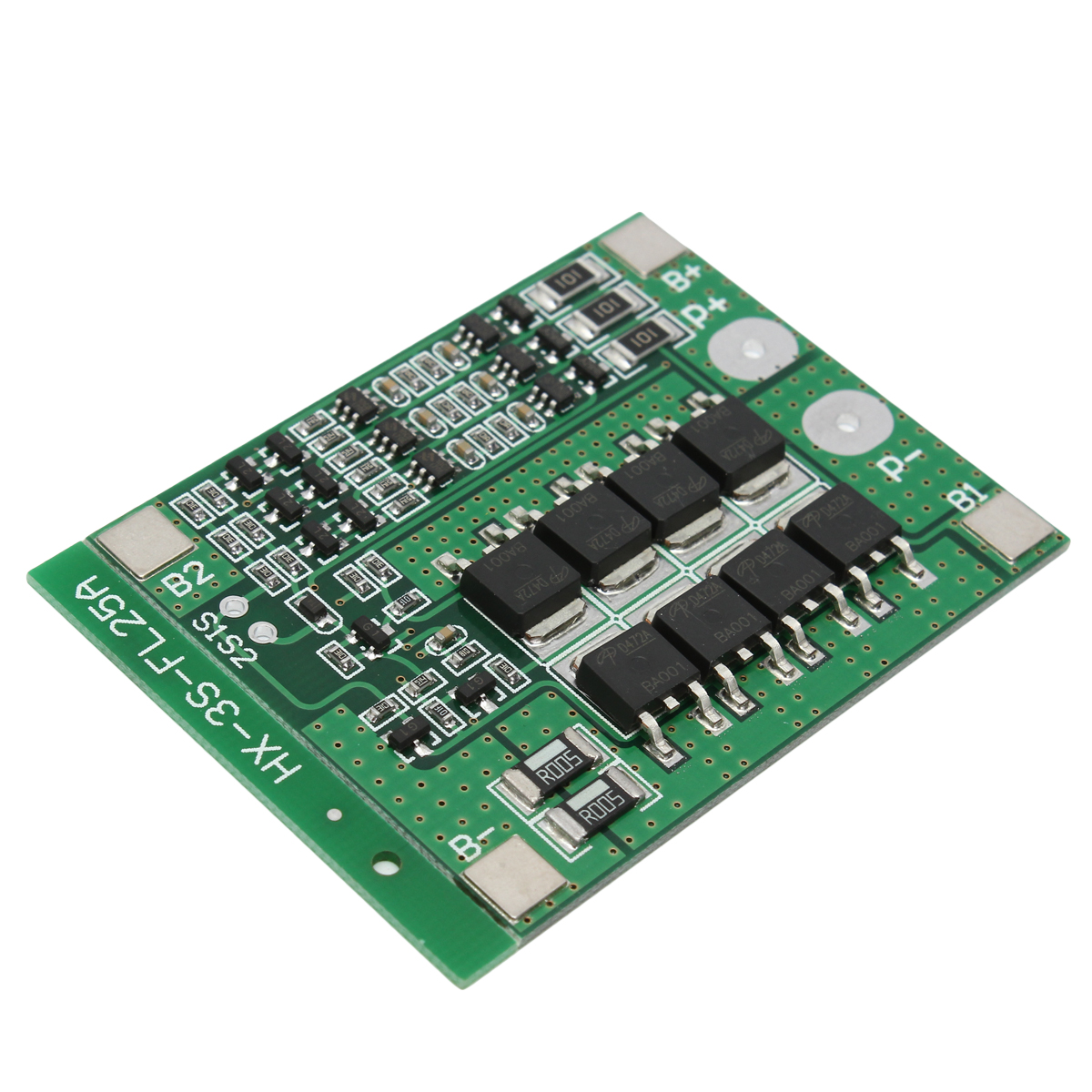
A PCB Board
II Prevention of PCB Warping During Processing
2.1 Prevent the Warping Due to Improper Inventory Mode
2.1.1 During the storage, the warping of the copper clad laminate will increase due to its absorption of moisture. For the single-sided copper clad laminate, its moisture absorption area is large, if the humidity in the inventory environment is too high, its warping will significantly increase. And for the double-sided copper clad laminate, moisture can only penetrate from the end face of the product, so the moisture absorption area is small, and the warping changes slowly. Therefore, for the copper clad laminate without moisture-proof packaging, manufactures should pay attention to the conditions of warehouse, minimize the humidity of warehouses to avoid the increase of the warping of the copper clad laminate during storage.
2.1.2 Improper Placement of Copper Clad Laminate will Increase warping.
Being set up tight, pressed with heavy objects, in poor placement, etc. will increase the deformation of copper plate.
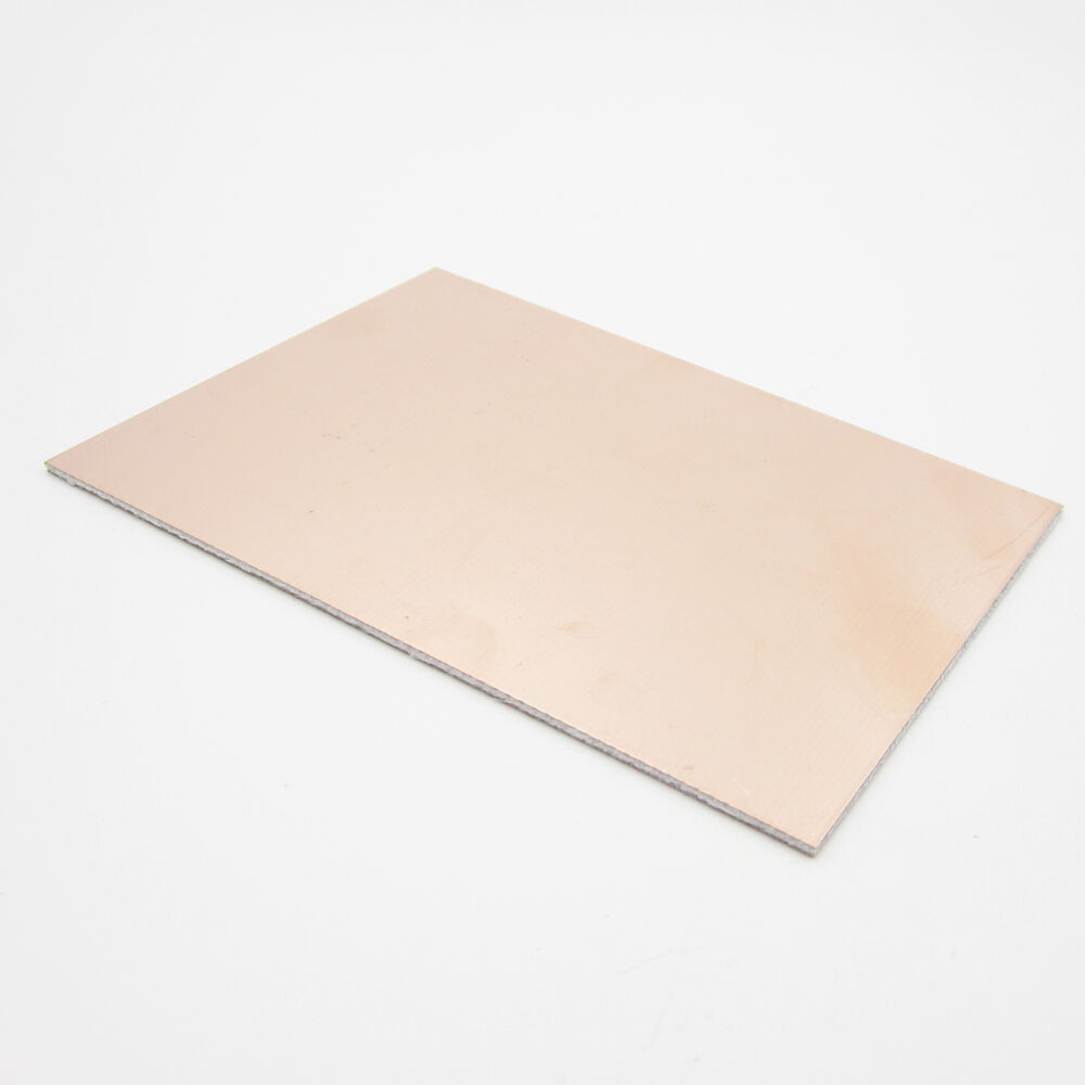
A Copper Clad Laminate
2.2 Avoid Warping Caused by Improper Design or Improper Processing
If the PCB board conducting circuit pattern is unbalanced or the PCB board is obviously asymmetrical on both sides, there will be a large area of copper skin on one side, which forms a large stress, causing the PCB board to warp. In addition, high processing temperature or large thermal shock during the processing of the PCB board will also cause the warping.
For the influence of improper inventory mode, the factory can easily solve the problem by improving the storage environment and avoiding vertical placement and heavy pressure. However, for PCB boards with a large area of copper skin, it is best to mesh the copper foil to reduce stress.
2.3 Eliminate Stress on Substrate
During the processing of the PCB board, the substrate is heated for many times and is subjected to various chemical substances. For example, after the substrate is etched, it should be washed, dried, and heated. In the process of pattern plating, the plating is usually hot. After printing the green oil and characters of logos, the PCB board should be dried or heated with UV light. And during the process of solder coating with hot air, the substrate will receive a great thermal shock. All these processes aforementioned can cause warping of the PCB board.
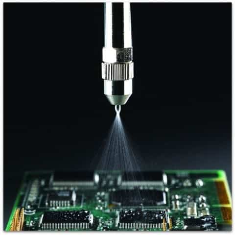
Solder Coating of PCB Boards
2.4 Baking Board
Since stress is the main cause of substrate warping, many PCB factories will bake the board before the copper clad laminate is used, which is considered to beneficial to reduce the warping of the PCB board. Baking plate can sufficiently relax the stress of the substrate, thereby reducing the deformation of the substrate in the production of PCB boards.
Big PCB board factories usually use large ovens to dry the boards. Before being put into production, a large stack of copper clad laminates will be put into the oven, and baked for several hours at a temperature near the glass transition temperature of the substrate. The PCB boards made by the baked copper clad laminate will has a small warping deformation, and the qualification rate will be much higher. For some small PCB board factories, if there is not such a large oven, the substrate can be cut into smaller chunks before baking. During the process of baking, an object should be pressed against the plate to keep the balance of the substrate during the stress relaxation process. Baking temperature should be neither too high nor too low. The substrate will easily change color when the temperature is too high, and if the temperature is too low, it will take a longer time to relax the substrate stress.
![]()
Position of the Substrate
III Leveling Method of PCB Warping
3.1 Level Warping in time in the Production of PCB Boards
In the production process of PCB board, pick out boards with large warping and level the warping with a rolling leveler, and then put the boards into the next process. Many PCB board manufacturers believe that this method is effective for reducing the warping ratio of finished PCB boards.
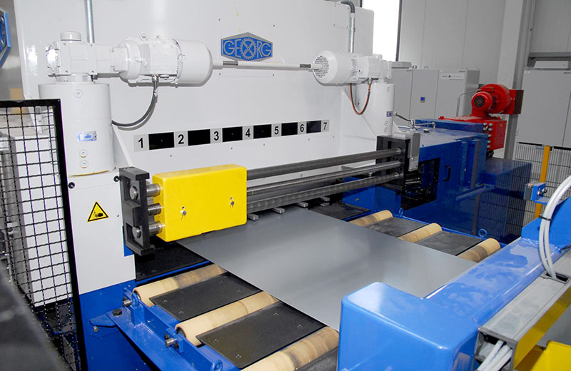
A Rolling Leveler
3.2 Leveling Method of Finished PCB Warping
For the finished PCB boards with the obvious warping that can not be leveled by the rolling lever, Some factories try to put them into a subpress (similar to a gripper) and level them for several hours with cold pressing. However, this method is not very effective, for the effect of leveling is not great, and the leveled board is easy to rebound (ie, the warping is recovered).
While some other factories will first heat the subpresser to a certain temperature, then level the warped PCB boards with hot pressing, of which the effect will be better than the cold pressing. However, if the pressure is too large, the wire will be deformed; and overtemperature will cause the discoloration of the rosin water.
Whether it is cold-pressing leveling or hot-pressing leveling, it will takes a long time (a few hours to over ten hours) to take effects, and the proportion of warping rebound of the leveled PCB boards is high. Is there a better leveling method?
3.3 Hot-pressing Leveling Method with an Arc Mold
According to the mechanical properties of polymer materials, the hot-pressing leveling method is recommended. Here are two kinds of operating methods:
3.3.1 Oven-baking Leveling Method
Make the warped surface of the PCB board facing the curved surface of the arc mold, and adjust the screw to deform the PCB board slightly in the opposite direction of the warping, and then then put the arc mold with the PCB board placed in it into a oven, of which the temperature has been heated to a certain temperature, to be baked for a while. Under the heated condition, the stress of the substrate gradually relaxes, restoring the deformed PCB board to a flat state. However, the baking temperature should not be too high, so as to prevent the discoloration of the rosin water or the yellowing of substrate. However, the temperature should also not be too low, or it will take a long time to completely relax the stress at a low temperature.
Generally, the glass transition temperature of the substrate can be used as the reference temperature for baking. It is also the phase transition point of the resin, at which the polymer segments can be rearranged to sufficiently relax the substrate stress, and the leveling effect is obvious. Leveling with the arc mold only needs small investment. The ovens are all available in the PCB board factories. The leveling operation is very simple. And If the number of warped boards is relatively large, making a few more arc molds is enough. Besides, several molds can be put into a oven at a time, and the baking time is relatively short (about dozens of minutes), so the leveling efficiency is relatively high.
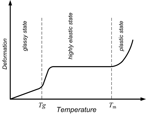
Glass Transition Temperature
3.3.2 Compression Leveling Method
For PCB boards with a small warping deformation, first put the, into an oven that has been heated to a certain temperature determined by the glass transition temperature of the substrate. After baking the boards for a certain period of time, take out several boards and clip them into the arc mold. Then adjust the screw, and make the boards slightly deformed in the opposite direction of its warping. After the board is cooled and shaped, the mold can be removed and the leveled PCB boards can be taken out.
In addition, it’s better to perform several small tests in advance to determine the baking temperature and baking time of the leveling. If the baking time is longer, the substrate is well-baked, thus the leveling effect will be better, and there will be less warping rebound of the PCB boards.
After the leveling with the arc mold, the warping rebound rate of the PCB boards is much lower, and the change of the color of the PCB board is small. And even after wave soldering, PCB board can still maintain a flat state.
IV Conclusion
PCB warping is a“headache”for all the PCB board factories, which not only reduces the yield but also affects the time of delivery. If the arc-shaped mold is used for hot-pressing leveling with a reasonable and suitable leveling process, the warped PCB board can be perfectly leveled, thus effectively solving the problem of yield and delivery date aforementioned.
You May Also Like:
Core Issue When Designing a PCB: Power-on
Structures and Applications of the FPCB
Copying the Board, How Should I Copy It?
Ordering & Quality
| Photo | Mfr. Part # | Company | Description | Package | Qty |
|
P87C554SBAA,512 | Company:NXP | Remark:IC MCU 8BIT 16KB OTP 68PLCC | Package:68-LCC (J-Lead) |
P87C554SBAA,512 Datasheet |
In Stock:510 Inquiry |
Inquiry |
|
DSPB56374AE | Company:NXP / Freescale | Remark:IC DSP 24BIT 150MHZ 52-LQFP | Package:52-LQFP |
DSPB56374AE Datasheet |
In Stock:10211 Inquiry |
Inquiry |
|
MC908JL8MDWE | Company:NXP / Freescale | Remark:IC MCU 8BIT 8KB FLASH 28SOIC | Package:28-SOIC (0.295", 7.50mm Width) |
MC908JL8MDWE Datasheet |
In Stock:1023 Inquiry |
Inquiry |
|
TMS320DM8127SCYED3 | Company:Texas Instruments | Remark:IC DGTL MEDIA PROCESSOR | Package:684-BFBGA, FCBGA |
TMS320DM8127SCYED3 Datasheet |
In Stock:433 Inquiry |
Inquiry |
|
A3P030-1QNG48I | Company:Microsemi | Remark:IC FPGA 34 I/O 48QFN | Package:48-VFQFN Exposed Pad |
A3P030-1QNG48I Datasheet |
In Stock:146 Inquiry |
Inquiry |
|
MPC8280VVQLDA | Company:NXP / Freescale | Remark:IC MPU MPC82XX 333MHZ 408TBGA | Package:480-LBGA |
MPC8280VVQLDA Datasheet |
In Stock:744 Inquiry |
Inquiry |
|
MPC8548EVTAUJC | Company:NXP / Freescale | Remark:IC MPU MPC85XX 1.333GHZ 783BGA | Package:783-BBGA, FCBGA |
MPC8548EVTAUJC Datasheet |
In Stock:842 Inquiry |
Inquiry |
|
MC68882CFN25A | Company:NXP | Remark:- | Package:PLCC68 |
MC68882CFN25A Datasheet |
In Stock:115 Inquiry |
Inquiry |
|
K9F4G08UOA-P1BO | Company:SAMSUNG | Remark:4G-bit NAND Flash Memory with spare 128M-bit | Package: |
K9F4G08UOA-P1BO Datasheet |
In Stock:5960 Inquiry |
Inquiry |
|
CM2020-00TR | Company:ON Semiconductor | Remark:IC HDMI TX PORT P/I 38-TSSOP | Package:38-TFSOP (0.173", 4.40mm Width) Exposed Pad |
CM2020-00TR Datasheet |
In Stock:183990 Inquiry |
Inquiry |