1
Printed circuit board {PCB circuit board, is the provider of electrical connections for electronic components. It has been developed for more than 100 years; its design is mainly layout design; the main advantage of using the circuit board is that it greatly reduces wiring and assembly errors, and improves the automation level and production labor rate. This article mainly introduces the manufacturing process of PCB from 10 steps. Let's take a look at this article.
Catalog
I PCB Layout | |
II The Core Board Manufacture | |
III The Transfer of Inner PCB Layout | |
IV Inner Core Board Etching | |
V Drilling Hole and Inspection of the Core Board | |
VI Lamination | |
VII Drilling Hole | |
VIII Copper Chemical Precipitation of Hole Walls | 1. Fixing |
2. Cleaning | |
3. Shipping | |
IX The Chemical Precipitation of Copper Film | 1. The Transfer of the outer PCB Layout |
2. Fixing PCB | |
3. Computer Control and Copper Plating | |
X Outer PCB Board Etching | 1. Clean out the cured photosensitive film on PCB board. |
2. Clean out the unwanted copper foil covered by PCB board with strong base. | |
3. Remove the tin plating on the PCB layout copper foil with tin-fading liquid. | |
4. Clean it out. | |
I PCB Layout
Firstly, sort out and check the PCB layout. Because each CAD software has its own unique file format, so PCB manufacture factory will be converted into a unified format - Extended Gerber RS-274X or Gerber X2 when it receives the CAD files from the PCB design company.
Secondly, the factory engineers will check whether the PCB layout conforms to the manufacturing process and whether there are any defects or other problems.
.gif")
In one issue of homemade PCB information, it mentions that the PCB layout is printed on paper with a laser printer and then transferred to a copper clad laminate(CCL).However, in the printing process, since the printer is prone to ink breakpoints, it is necessary to manually fill the ink with an oil-based pen.

A small amount of production is OK, but if this defect is transplanted to industrial production, it will greatly reduce production efficiency. So, the factory generally uses a photocopying method to print the PCB layout on the film. If it is a multi-layer PCB board, the printed layout film on each layer will be arranged in order.

The film will then be aligned. It is important to align the holes, and then depends on the alignment holes in order to align the material of each layer of the PCB.

II The Core Board Manufacture
Clean out the copper clad laminate, and if there is dust on it, it may cause the last circuit to be short-circuited or broken.

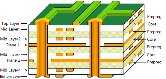
The figure below is an illustration of an 8-layer PCB. It is actually made up of 3 copper clad laminates (core boards) and 2 sheets of copper films, which are bonded together with prepregs.
III The Transfer of Inner PCB Layout
Firstly, make the two-layer circuits of the most middle core board. After the copper clad laminate is cleaned, it will be covered with a photosensitive film on the surface. This film will solidify when exposed to light, forming a protective film on the copper foil of the copper clad laminate.

Secondly, insert two layers of PCB layout film and double-layer copper clad laminates into the upper layer of PCB layout film to ensure accurate stacking position of the upper and lower PCB layout films.

Thirdly, the copper foil covered under the cured photosensitive film is the needed PCB layout circuit, which is equivalent to the function of the laser printer ink of the manual PCB. In the paper PCB layout of the previous laser printer, the black toner under the cover was the copper foil to be retained. In this period, the copper foil covered by the black film will be corroded, while the transparent film will be retained because the photosensitive film is cured.

Lastly, wash the uncured photosensitive film with lye, and the required copper foil circuits will be covered by the cured photosensitive film.

IV Inner Core Board Etching
Use the strong base, such as NaOH to etch away the copper foil not needed.

Tear off the cured photosensitive film to expose the needed PCB layout circuit copper foil.

V Drilling Hole and Inspection of the Core Board
After the core board is successfully made, then the alignment holes are made on the core board to facilitate alignment with other raw materials.

Once the core board is pressed together with the other layers of PCB, it cannot be modified, so the inspection is very important. The machine will automatically compare with the PCB layout drawing to check the errors.
The first two layers of PCB board have been made.
VI Lamination
A new material called a prepreg is needed here, which is the adhesive between the core board and the core board (>2 layers of PCB), and between the core board and the outer layer of copper foil, and also plays an insulating role.

The lower layer of copper foil and the two layers of prepreg have been fixed in advance through the alignment hole and the iron plate in the lower layer, and then the prepared core plate is put into the alignment hole. Finally cover the two layers of prepregs, one layer of copper foil and one layer of pressure-bearing aluminum plate on the core board in turn.

In order to improve work efficiency, the factory will stack 3 different PCB boards together and then fix them. The upper iron plate is sucked by magnetic force, which is convenient for alignment with the lower iron plate.
After the two layers of iron plates are aligned successful by inserting the alignment pins, the machine compresses the space between the iron plates as much as possible, and then fixes them with nails.

Place the PCB boards clamped by iron plates on the bracket and then sent them into a vacuum hot press for lamination. The high temperature in the vacuum hot press can melt the epoxy resin in the prepreg and fix the core boards and copper foils together under pressure.


After the lamination is completed, remove the upper iron plate that presses the PCB . Then remove the pressure-bearing aluminum board which serves to isolate the different PCBs and ensure the smoothness of the outer copper foil of the PCB. Both sides of the PCB taken out at this time will be covered by a layer of smooth copper foil. At the moment, both sides of the PCB will be covered with a smooth layer of copper foil.

VII Drilling Hole
Firstly, drill through holes from top to bottom to get through the PCB, and then metallize the hole wall to conduct electricity.

Locate the inner core board with the X-ray drilling machine. The machine will automatically find and locate the hole on the core board, and then drill location hole on the PCB to ensure that the next hole is drilled through the right center of the hole.

Place a layer of aluminum plate on the drilling machine, and then place the PCB on it. Because drilling is a bit slow process, in order to improve efficiency, 1 to 3 identical PCB boards will be stacked together for perforation according to the number of PCB layers. Finally, cover an aluminum plate on the top PCB. The upper and lower layers of the aluminum plate are designed to avoid tearing the copper foil on the PCB when the drill bit is drilled in and out.

Next, the operator only needs to select the correct drilling program, and the rest is done automatically by the drilling machine. The drill bit is driven by air pressure with a maximum rotation of 150000 revolutions per minute, which is enough to ensure the smoothness of the hole wall.

The replacement of the drill bit is also done automatically by the machine according to the program. The smallest bit can reach 100 microns in diameter, while the human hair is 150 microns in diameter.

In the previous lamination process, the melted epoxy resin was extruded outside the PCB, so it needed to be removed. And the die milling machine cuts its periphery according to the correct XY coordinates of PCB.


VIII Copper Chemical Precipitation of Hole Walls
Since nearly all PCB designs connect different layers of circuits by using perforations, a good connection needs 25 microns copper films on the hole wall. It needs to go through plating to reach such a thick copper film, but the hole wall is made up of non-conductive epoxy resin and fiberglass sheet. So the first step is to deposit a layer of conductive material on the hole wall and then form a 1 micron copper film on the whole surface of the PCB as well as the hole wall by chemical deposition. The whole process, such as chemical treatment and cleaning, is controlled by the machine.

1. Fixing

2. Cleaning PCB

3. Shipping

IX The Chemical Precipitation of Copper Film
1. The Transfer of the outer PCB Layout
The outer PCB layout will be transferred to the copper foil, and the process is similar to the principle of the previous inner core PCB layout transfer. Both of the two processes transfer PCB layout to copper foil through using photocopied film and photosensitive film, and the only difference is that it uses the positive film to make the board now.
The previous transfer of inner core PCB layout adopts subtraction method, which uses the negative film to make the board. The circuit is covered by the cured photosensitive film on the PCB. After cleaning away the uncured photosensitive film, the exposed copper foil is etched, the PCB layout circuit is protected by the cured photosensitive film and then is retained. The transfer of outer layer of PCB layout is the normal method, which uses positive film to make board. The non-circuit area is covered by cured photosensitive film on PCB. Plating is performed after cleaning off the uncured photosensitive film. Where there is a film, it cannot be plated, but where there is no film, copper is first plated and then tin is plated. After the film is removed, the alkaline etching is performed, and the tin was finally removed. The circuit pattern remains on the board because it is protected by tin.
Put the PCB whose both sides of copper foil have been cleaned into the laminator, and then the laminator presses the photosensitive film onto the copper foil.

Fix the two layers of photocopying PCB layout film through the location hole, and place the PCB board into the middle. And then cure the photosensitive film, which is the circuit needs to be retained, under the transparent film by the irradiation of a UV lamp.


Clean out the photosensitive film that is not needed and cured, and then check it out.


Clamp PCB with a clip, and then plate copper on it. As mentioned earlier, in order to ensure good enough conductivity of the hole, the copper film on the hole wall must be 25 microns thick, so the whole system will be automatically controlled by computer to ensure its accuracy.

2. Fixing PCB

3. Computer Control and Copper Plating
After the copper film plating is completed, the computer will also arrange for plating another thin layer of tin.

Unload the tinned PCB and then check it to ensure that the thickness of the plated-copper and plated-tin is correct.


X Outer PCB Board Etching
Next, the etching process is a complete automated pipeline.
1. Clean out the cured photosensitive film on PCB board.

2. Clean out the unwanted copper foil covered by PCB board with strong base.

3. Remove the tin plating on the PCB layout copper foil with tin-fading liquid.

4. Clean it out.

The 4-layer PCB layout is completed.
You May Also Like:
Prevention and Leveling Method of the Warping in PCB Production
Structures and Applications of the FPCB
A Core Issue When Designing a PCB: Power-on
Copying the Board, How Should I Copy It?
Ordering & Quality
| Photo | Mfr. Part # | Company | Description | Package | Qty |
|
LFE2-6SE-5FN256C | Company:Lattice Semiconductor | Remark:IC FPGA 190 I/O 256BGA | Package:256-BGA |
LFE2-6SE-5FN256C Datasheet |
In Stock:270 Inquiry |
Inquiry |
|
MCIMX507CVM8B | Company:NXP / Freescale | Remark:IC MPU I.MX50 800MHZ 400MAPBGA | Package:400-LFBGA |
MCIMX507CVM8B Datasheet |
In Stock:607 Inquiry |
Inquiry |

|
MAX1490AEPG+ | Company:MAXIM | Remark:IC RS485/RS422 DATA INTRFC 24DIP | Package:PDIP-24 |
MAX1490AEPG+ Datasheet |
In Stock:8428 Inquiry |
Inquiry |
|
MC68360ZQ25L | Company:Freescale Semiconductor - NXP | Remark:IC MPU M683XX 25MHZ 357BGA | Package:BGA |
MC68360ZQ25L Datasheet |
In Stock:811 Inquiry |
Inquiry |
|
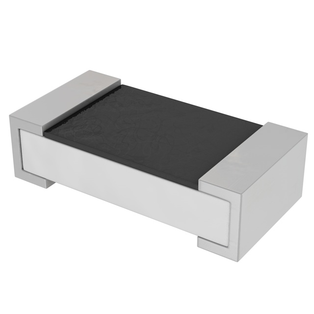
RC0603FR-071KL | Company:Yageo | Remark:RES SMD 1K OHM 1% 1/10W 0603 | Package:SMD |
RC0603FR-071KL Datasheet |
In Stock:39061200 Inquiry |
Inquiry |
|
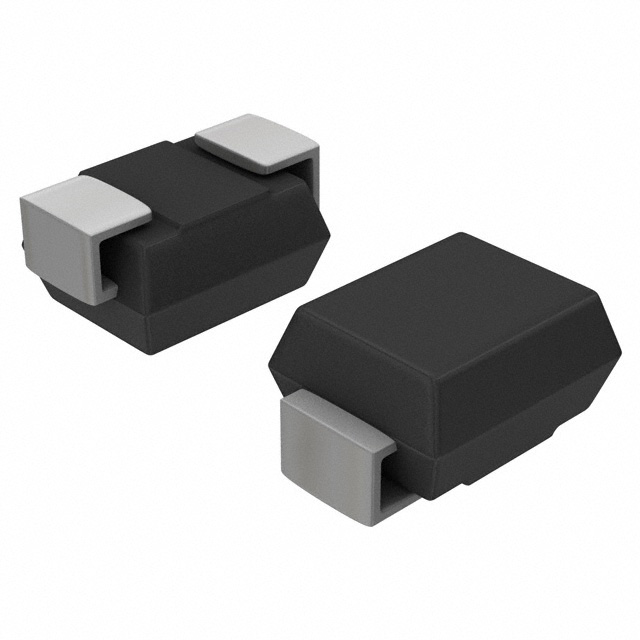
MBRS130LT3G | Company:ON Semiconductor | Remark:DIODE SCHOTTKY 30V 2A SMB | Package:SMB |
MBRS130LT3G Datasheet |
In Stock:516247 Inquiry |
Inquiry |
|
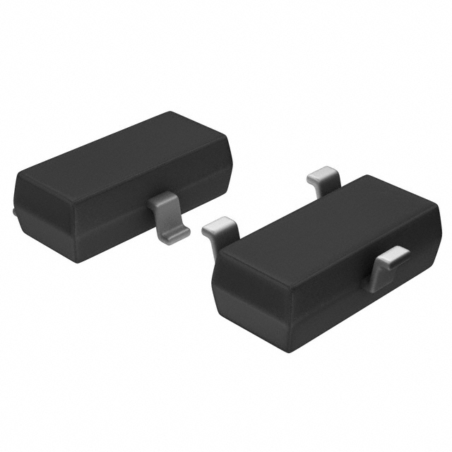
DS1816R-5+T&R | Company:Maxim Integrated | Remark:IC 3.06V OD 5% SOT23-3 | Package:TO-236-3, SC-59, SOT-23-3 |
DS1816R-5+T&R Datasheet |
In Stock:7060 Inquiry |
Inquiry |
|
BCM7501KFB P20 | Company:BROADCOM | Remark:IC Chips | Package:BGA64 |
BCM7501KFB P20 Datasheet |
In Stock:19250 Inquiry |
Inquiry |
|
FLC10-200H | Company:STMicroelectronics | Remark:IC FIRE LIGHTER CIRCUIT I-PAK | Package:TO-251-3 Long Leads, IPak, TO-251AB |
FLC10-200H Datasheet |
In Stock:5153 Inquiry |
Inquiry |

|
MC9S08QD4CSC | Company:NXP | Remark:IC MCU 8BIT 4KB FLASH 8SOIC | Package:SOIC8 |
MC9S08QD4CSC Datasheet |
In Stock:41393 Inquiry |
Inquiry |