6
Catalog
I Introduction |
II Board Copying Techniques |
I Introduction
Speaking of copying board, you may feel that there is no technical content, and the people who have really copied should have a deep understanding -- this is not that simple.
PCB copying board has no software, so it can only be measured and drawn with caliper edge, which it's very slow and its accuracy is also poor. However, It is very easy to copy the board with the software. Generally, it is more convenient to use the board copying software of delta company. You can scan or take a picture of the PCB board first, and then load the picture into the software according to the gourd drawing ladle. But it's more difficult to transform the PCB diagram into schematic diagram, because it needs experience and knowledge, otherwise, it can't be completed successfully.
It is more troublesome to copy the multi-layer board, because the inner layer cannot be seen, so we can only damage the sample. Generally, we cope on the top and bottom first, and then keep the bottom and the top down in front of the photo (for reference). Beside, a accurate method is to dismantle all components, and then register all components parameters, and number one by one of the components and silkscreen layer corresponding to retain the original information, or scan again to bare PCB photography, get photos or scan in software. Different software has different requirements, like the size of photo, if the size is too big, it will have a effect on the the speed of copy board. So too big PCB copy board can be divided into several small pieces, then split. After the upper and lower layers are completed, the finished layer can be polished with sandpaper to gradually expose the inner layer, copy one layer and then grind the next layer until all is completed.
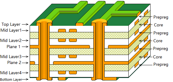
Multi-layer Board
II Board Copying Techniques
Nowadays, there are a number of well-known companies in the industry that can help you copy those complex PCB boards. For some relatively simple circuit boards, it is also a very valuable experience to copy them by yourself. Today I'm going to tell you a little about the board copying technique.
Equipment required: scanners, computers, PORTEL99 and AUTOCAD.
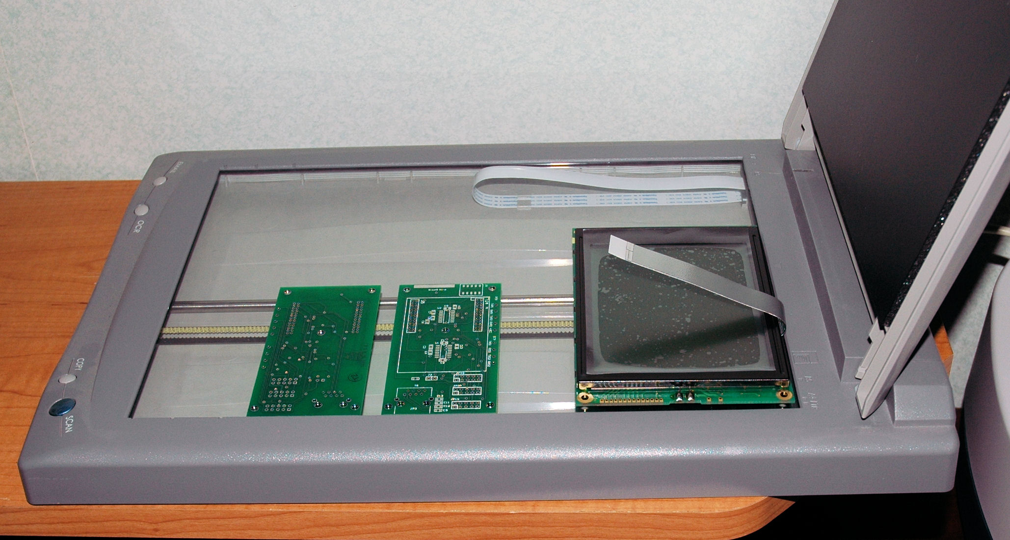
1. Put the PCB board that you want to copy into the scanner, and start the scanner, pay attention to adjust the brightness and contrast in the scanner.
2. Open AUTO CAD software, and create a new CAD file, and select the insert raster image from the insert menu. After selecting the image that you want to insert, the insert image dialog box will appear.
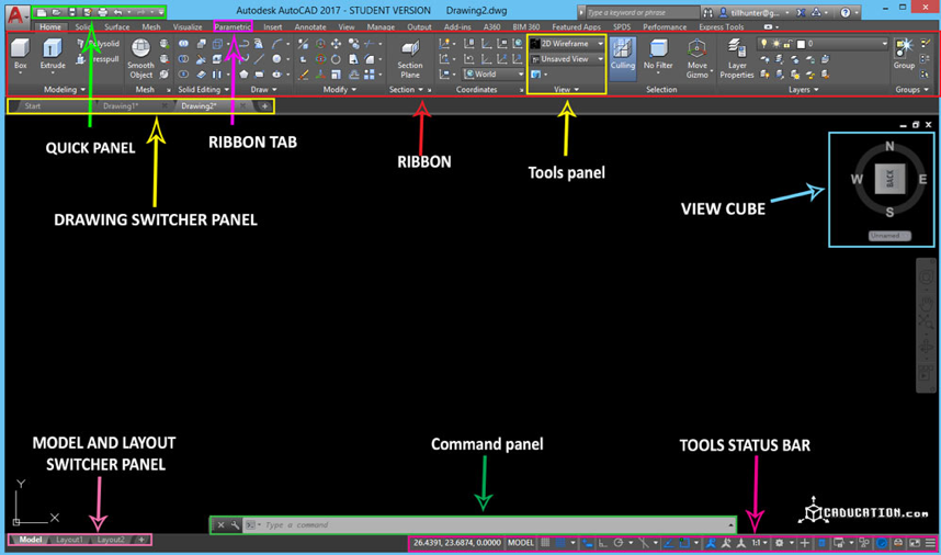
Interface of Auto Cad
3. After you insert the PCB image, you should draw a rectangular frame to cover the border of the PCB. Note that the object lock point for tracking should be used when you draw the border. If you do not draw the border, you will get trouble when you draw the circuit diagram and made it moved carelessly.
4. Draw component package. We need to establish component package by ourselves, and that's because the component package we copied in the PCB is different from the component package in the PORTEL99. It means we have to draw the PCB components shape, and then we need to count how many packages are used on the PCB board when we are drawing component package. Every package just needs to draw one, and after drawing all of them, we will transfer them to the PORTEL 99 again for processing.
5. Open PORTEL99, first create a new PCB file, and then choose to import CAD file from the file menu of PORTEL99 PCB editor. Guide the CAD file of the component model into it. After successful import, the basic graph of component packaging appears in the PORTEL99 PCB editor.
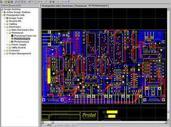
Interface of Portel99
6. Create a new PCB component editor in PORTEL99 and open the PCB component editor. After creating a new component, select a component from the PORTEL99 PCB editor package and copy it to the PCB component editor for making the component.
7. When all the component packages are finished, place them in the PORTEL99 PCB editor and export them to a CAD file.
8. After opening the CAD file of the component package drawing, the CAD file that was previously imported into the PCB picture is also opened, and the component package drawing is copied to the CAD with the PCB picture. At this time, the CAD file of only the component package drawing can be closed. It is necessary to work in a CAD file with a PCB picture. According to the arrangement angle and position of the components of the PCB diagram, the components are arranged in turn, and more sub-components are made by copying and pasting.
8. Place the pads and vias. First measure the inner and outer diameters of the pads in the CAD, then select the circle sub-item in the drawing menu. And determine the inner and outer diameter of the ring. When placing the pad, the pad of the same size should be discharged at one time, but the square pad and the polygon pad cannot be placed, although the method of filling in CAD will be used. The polygon fills in the solid, but the filled entity will only have an empty border when it goes inside PORTEL 99. Therefore, if there is a polygon pad in the PCB, we can use the line to trace the edge of the pad and go to PORTEL99. Then put the corresponding pads.
Via in Pad
9. Draw the trace. The draw trace is drawn by the aggregate line. In the drawing menu, select the aggregate line, determine the start width and end width of the aggregate line, and then start drawing. In the drawing process, if it is a straight line, it is necessary to select the orthogonal trace. If it is 45 degrees or other angles, the orthogonal trace should be canceled. If the width of the middle line of the whole circuit board is only a few specifications, we can also Use ordinary lines to draw, but different line widths use different layers, go to PORTEL 99 and edit the line width.
10. When the line is completed, we carry out the last work in the CAD, place the silk screen, if it is text, use the method of placing the text box. If it is irregular silk screen, use the polymer line, of course you also To draw directly with lines, go to PORTEL 99 and edit the line width.
11. After the above steps, the work in CAD has been basically completed. If you don't go to PORTEL, you can also ask the PCB dealer to help you with the board. You can also print out the layers you need and make PCBs yourself. Of course, the ultimate goal of my writing is to tell the reader to transfer the depicted graphics to PORTEL, so we'll continue with the next few steps.
12. Open the PORTEL99 PCB editor and import the CAD files you have already drawn. Note that it is important to map the various layers of CAD to the various layers of PORTEL99 in the dialog box for importing files, regardless of the name of the layer in your CAD. What is it, but you must know what layer this layer responds to in PORTEL99. If you do not control the chaos, you will spend more time on the PORTEL 99 layer conversion, and also import the default. The line width is also best changed.
13. Last edit, after importing PORTEL99, we need to make proper editing. For example, when we import, we put the lines and pads on the TOP LAYER layer. At this time, you should put all the pads on the MULTI LAVER layer, and No matter which angle you put the silkscreen text in CAD, you will be corrected when you go to PORTEL 99. At this time, you have to adjust it against the physical PCB.
14. If there is another line or silk screen, just follow the above method, then lead to PORTEL 99 integration, pay attention to mirroring. Finally, check the image or PCB carefully, you can also make appropriate modifications and you're done. It is.
Precautions
If you accidentally move the picture in CAD, then all the lines you draw will be invisible. At this time, you have to remove all the pictures, and then select all the lines you have drawn
You May Also Like:
Prevention and Leveling Method of the Warping in PCB Production
Structures and Applications of the FPCB
A Core Issue When Designing a PCB: Power-on
Ordering & Quality
| Photo | Mfr. Part # | Company | Description | Package | Qty |
|
73M2R010F | Company:CTS Electronic Components | Remark:RES SMD 0.01 OHM 1% 2W 2512 | Package:2512 J-Lead |
73M2R010F Datasheet |
In Stock:1263 Inquiry |
Inquiry |
|
MCF52210CEP66 | Company:NXP | Remark:IC MCU 32BIT 64KB FLASH 64QFN | Package:64-VFQFN Exposed Pad |
MCF52210CEP66 Datasheet |
In Stock:144 Inquiry |
Inquiry |
|
MAX811SEUS-T | Company:Maxim Integrated | Remark:IC MPU V-MONITOR 2.93V SOT143-4 | Package:TO-253-4, TO-253AA |
MAX811SEUS-T Datasheet |
In Stock:33630 Inquiry |
Inquiry |
|
BCM5221KPB | Company:Broadcom Limited | Remark:Ethernet ICs 10/100Base TX/FX Mini-PH Tra | Package:BGA |
BCM5221KPB Datasheet |
In Stock:975 Inquiry |
Inquiry |
|
MMA8451QR1 | Company:Freescale Semiconductor - NXP | Remark:ACCELEROMETER 2-8G I2C 16QFN | Package:QFN |
MMA8451QR1 Datasheet |
In Stock:25194 Inquiry |
Inquiry |
|
BCM7501KFB P20 | Company:BROADCOM | Remark:IC Chips | Package:BGA64 |
BCM7501KFB P20 Datasheet |
In Stock:19250 Inquiry |
Inquiry |
|
MC68360ZQ25L | Company:Freescale Semiconductor - NXP | Remark:IC MPU M683XX 25MHZ 357BGA | Package:BGA |
MC68360ZQ25L Datasheet |
In Stock:811 Inquiry |
Inquiry |
|
MC68HC908LK24CFU | Company:NXP | Remark:IC MCU 8BIT 24KB FLASH 64QFP | Package:64-QFP |
MC68HC908LK24CFU Datasheet |
In Stock:3071 Inquiry |
Inquiry |
|
A3P030-1QNG48I | Company:Microsemi | Remark:IC FPGA 34 I/O 48QFN | Package:48-VFQFN Exposed Pad |
A3P030-1QNG48I Datasheet |
In Stock:146 Inquiry |
Inquiry |
|
TMS320DM6433ZWTQ5 | Company:Texas Instruments | Remark:IC DGTL MEDIA PROCESSOR 361-BGA | Package:361-LFBGA |
TMS320DM6433ZWTQ5 Datasheet |
In Stock:485 Inquiry |
Inquiry |