| Manufacturer Part#: | A3P030-1QNG48I |
| Product Category: | Embedded - FPGAs (Field Programmable Gate Array) |
| Manufacturer: | Microsemi |
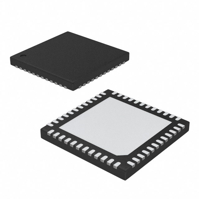
| Description: | IC FPGA 34 I/O 48QFN |
| Package: | 48-VFQFN Exposed Pad |
| Quantity: | 146 PCS |
| Lead Free Status / RoHS Status: | Lead free / RoHS Compliant |
| one to seven days | |
| Click buy button to purchase: | Buy |
CAD Models

A3P030-1QNG48I Symbol

A3P030-1QNG48I Footprint
Lifecycle Status Indicator

A3P030-1QNG48I Lifecycle Status Indicator
Product Attributes
Manufacturer | Microsemi Corporation |
Product Category | Embedded - FPGAs (Field Programmable Gate Array) |
Series | ProASIC3 |
Brand | Microsemi |
EU RoHS | Compliant |
ECCN (US) | EAR99 |
JESD-30 Code | S-XQCC-N48 |
JESD-609 Code | e3 |
Mounting Style | SMD/SMT |
Mounting Type | Surface Mount |
Maximum Operating Temperature | 100 °C |
Minimum Operating Temperature | -40 °C |
Maximum Voltage Supply | 1.575 V |
Normal Supply Voltage | 1.5 V |
Minimum Voltage Supply | 1.425 V |
Maximum Operating Frequency | 272 MHz |
Maximum I/O Performance | 700Mbps |
Maximum Reflow Temperature | 260 °C |
Number of Gates | 30000 |
Number of I/O | 34 |
Number of I/O Banks | 2 |
Number of Registers | 768 |
Number of Inter Dielectric Layers | 7 |
Number of Pins | 48 |
Number of CLBs | 768 |
Number of Inputs | 34 |
Number of Logic Cells | 768 |
Number of Outputs | 34 |
Number of Reflow Cycle | 3 |
Organization | 768 CLBS, 30000 GATES |
Operating Supply Current | 2 mA |
Package / Case | 48-VFQFN Exposed Pad |
Mfr Package Description | 8 X 8 MM, 0.90 MM HEIGHT, 0.40 MM PITCH, GREEN, QFN-48 |
Package Body Material | UNSPECIFIED |
Package Code | HQCCN |
Package Equivalence Code | LCC48,.24SQ,16 |
Package Shape | SQUARE |
Package Style | CHIP CARRIER, HEAT SINK/SLUG |
Peak Reflow Temperature (Cel) | 260 |
Power Supplies | 1.5,1.5/3.3 |
PCB changed | 48 |
Program Memory Type | Flash |
Programmable Logic Type | FIELD PROGRAMMABLE GATE ARRAY |
Reflow Solder Time (Sec) | 20 to 40 |
Seated Plane Height | 0.9 mm |
Speed Grade | 1 |
Sub Category | Field Programmable Gate Arrays |
Supplier Device Package | 48-QFN (6x6) |
Tradename | Actel |
Technology | CMOS |
Temperature Grade | INDUSTRIAL |
Terminal Finish | PURE TIN |
Terminal Form | NO LEAD |
Terminal Pitch | 0.4 mm |
Terminal Position | QUAD |
Time@Peak Reflow Temperature-Max | 30 s |
Lead Finish(Plating) | Matte Sn annealed|Au |
Under Plating Material | N/A|Pd over Ni |
Dimensions
Height | 0.88 mm |
Length | 6 mm |
Width | 6 mm |
Features and Benefits
◆ High Capacity
• 15 K to 1 M System Gates
• Up to 144 Kbits of True Dual-Port SRAM
• Up to 300 User I/Os
◆ Reprogrammable Flash Technology
• 130-nm, 7-Layer Metal (6 Copper), Flash-Based CMOS Process
• Instant On Level 0 Support
• Single-Chip Solution
• Retains Programmed Design when Powered Off
◆ High Performance
• 350 MHz System Performance
• 3.3 V, 66 MHz 64-Bit PCI†
◆ In-System Programming (ISP) and Security
• Secure ISP Using On-Chip 128-Bit Advanced Encryption Standard (AES) Decryption (except ARM-enabled ProASIC®3 devices) via JTAG (IEEE 1532–compliant)†
• FlashLock® to Secure FPGA Contents
◆ Low Power
• Core Voltage for Low Power
• Support for 1.5 V-Only Systems
• Low-Impedance Flash Switches
◆ High-Performance Routing Hierarchy
• Segmented, Hierarchical Routing and Clock Structure
◆ Advanced I/O
• 700 Mbps DDR, LVDS-Capable I/Os (A3P250 and above)
• 1.5 V, 1.8 V, 2.5 V, and 3.3 V Mixed-Voltage Operation
• Wide Range Power Supply Voltage Support per JESD8-B, Allowing I/Os to Operate from 2.7 V to 3.6 V
• Bank-Selectable I/O Voltages—up to 4 Banks per Chip
• Single-Ended I/O Standards: LVTTL, LVCMOS 3.3 V / 2.5 V / 1.8 V / 1.5 V, 3.3 V PCI / 3.3 V PCI-X† and LVCMOS 2.5 V / 5.0 V Input
• Differential I/O Standards: LVPECL, LVDS, B-LVDS, and M-LVDS (A3P250 and above)
• I/O Registers on Input, Output, and Enable Paths
• Hot-Swappable and Cold Sparing I/Os‡
• Programmable Output Slew Rate† and Drive Strength
• Weak Pull-Up/-Down
• IEEE 1149.1 (JTAG) Boundary Scan Test
• Pin-Compatible Packages across the ProASIC3 Family
◆ Clock Conditioning Circuit (CCC) and PLL†
• Six CCC Blocks, One with an Integrated PLL
• Configurable Phase-Shift, Multiply/Divide, Delay Capabilities and External Feedback
• Wide Input Frequency Range (1.5 MHz to 350 MHz)
◆ Embedded Memory†
• 1 kbit of FlashROM User Nonvolatile Memory
• SRAMs and FIFOs with Variable-Aspect-Ratio 4,608-Bit RAM Blocks (×1, ×2, ×4, ×9, and ×18 organizations)†
• True Dual-Port SRAM (except ×18)
◆ ARM Processor Support in ProASIC3 FPGAs
• M1 ProASIC3 Devices—ARM®Cortex™-M1 Soft Processor Available with or without Debug
General Description
ProASIC3, the third-generation family of Actel flash FPGAs, offers performance, density, and features beyond those of the ProASICPLUS® family. Nonvolatile flash technology gives ProASIC3 devices the advantage of being a secure, low-power, single-chip solution that is live at power-up (LAPU). ProASIC3 is reprogrammable and offers time-to-market benefits at an ASIC-level unit cost. These features enable designers to create high-density systems using existing ASIC or FPGA design flows and tools.
ProASIC3 devices offer 1 kbit of on-chip, reprogrammable, nonvolatile FlashROM storage as well as clock conditioning circuitry based on an integrated phase-locked loop (PLL). The A3P015 and A3P030 devices have no PLL or RAM support. ProASIC3 devices have up to 1 million system gates, supported with up to 144 kbits of true dual-port SRAM and up to 300 user I/Os. ProASIC3 devices support the ARM Cortex-M1 processor. The ARM-enabled devices have Actel ordering numbers that begin with M1A3P (Cortex-M1) and do not support AES decryption.
Diagram

A3P030-1QNG48I Diagram
Advantages and Disadvantages
There is no relevant information available for this part yet.
Applications
There is no relevant information available for this part yet.
Compliance
Radiation Hardening | No |
RoHS | Compliant |
Product Manufacturer
Microsemi Corporation (Nasdaq: MSCC) offers a comprehensive portfolio of semiconductor and system solutions for aerospace & defense, communications, data center and industrial markets. Products include high-performance and radiation-hardened analog mixed-signal integrated circuits, FPGAs, SoCs and ASICs; power management products; timing and synchronization devices and precise time solutions, setting the world’s standard for time; voice processing devices; RF solutions; discrete components; enterprise storage and communication solutions, security technologies and scalable anti-tamper products; Ethernet solutions; Power-over-Ethernet ICs and midspans; as well as custom design capabilities and services. Microsemi is headquartered in Aliso Viejo, Calif., and has approximately 4,800 employees globally.
Product Range
Audio & Voice | Circuit Protection | Drivers, Interfaces, and PCIe Switches |
Ethernet and PoE Solutions | FPGA & SoC | Optical Networking |
Power Discretes & Modules | Power Management | RF, Microwave & Millimeter Wave |
Distributors
Distributors | Stock | Manufacturers | Descriptions |
Kynix | 146 | Microsemi Corporation | IC FPGA 34 I/O 48QFN |
DigiKey | 0 | Microsemi Corporation | IC FPGA 34 I/O 48QFN |
Mouser | 0 | Microsemi | FPGA - Field Programmable Gate Array ProASIC3 |
Alternative Models
There is no relevant information available for this part yet.
Popularity by Region

A3P030-1QNG48I Popularity by Region
Market Price Analysis
There is no relevant information available for this part yet.
 IC FPGA 68 I/O 100VQFP
 IC FPGA 48 I/O 63WLCSP
 IC FPGA 500 I/O 900FCBGA