| Manufacturer Part#: | K9F4G08UOA-P1BO |
| Product Category: | Memory |
| Manufacturer: | SAMSUNG |
| Description: | 4G-bit NAND Flash Memory with spare 128M-bit |
| Package: | |
| Quantity: | 5960 PCS |
| Lead Free Status / RoHS Status: | Lead free / RoHS Compliant |
| one to seven days | |
| Click buy button to purchase: | Buy |
DESCRIPTION
Offered in 512Mx8bit, the K9F4G08U0A is a 4G-bit NAND Flash Memory with spare 128M-bit. Its NAND cell provides the most costeffective solution for the solid state application market. A program operation can be performed in typical 200µs on the (2K+64)Byte page and an erase operation can be performed in typical 1.5ms on a (128K+4K)Byte block. Data in the data register can be read out at 25ns cycle time per Byte. The I/O pins serve as the ports for address and data input/output as well as command input. The on-chip write controller automates all program and erase functions including pulse repetition, where required, and internal verification and margining of data. Even the write-intensive systems can take advantage of the K9F4G08U0A′s extended reliability of 100K program/ erase cycles by providing ECC(Error Correcting Code) with real time mapping-out algorithm. The K9F4G08U0A is an optimum solution for large nonvolatile storage applications such as solid state file storage and other portable applications requiring non-volatility.
APPLICATION
The K9F4G08U0A is a 4,224Mbit(4,429,185,024 bit) memory organized as 262,144 rows(pages) by 2,112x8 columns. Spare 64x8 columns are located from column address of 2,048~2,111. A 2,112-byte data register is connected to memory cell arrays accommodating data transfer between the I/O buffers and memory during page read and page program operations. The memory array is made up of 32 cells that are serially connected to form a NAND structure. Each of the 32 cells resides in a different page. A block consists of two NAND structured strings. A NAND structure consists of 32 cells. Total 1,081,344 NAND cells reside in a block. The program and read operations are executed on a page basis, while the erase operation is executed on a block basis. The memory array consists of 4,096 separately erasable 128K-byte blocks. It indicates that the bit by bit erase operation is prohibited on the K9F4G08U0A.
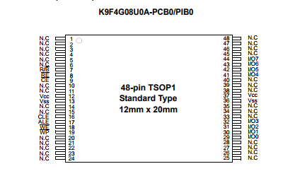
The K9F4G08U0A has addresses multiplexed into 8 I/Os. This scheme dramatically reduces pin counts and allows system upgrades
to future densities by maintaining consistency in system board design. Command, address and data are all written through I/O's by
bringing WE to low while CE is low. Those are latched on the rising edge of WE. Command Latch Enable(CLE) and Address Latch
Enable(ALE) are used to multiplex command and address respectively, via the I/O pins. Some commands require one bus cycle. For
example, Reset Command, Status Read Command, etc require just one cycle bus. Some other commands, like page read and block
erase and page program, require two cycles: one cycle for setup and the other cycle for execution. The 528M byte physical space
requires 30 addresses, thereby requiring five cycles for addressing : 2 cycles of column address, 3 cycles of row address, in that
order. Page Read and Page Program need the same five address cycles following the required command input. In Block Erase operation,
however, only the three row address cycles are used. Device operations are selected by writing specific commands into the command register. Table 1 defines the specific commands of the K9F4G08U0A.
In addition to the enhanced architecture and interface, the device incorporates copy-back program feature from one page to another page without need for transporting the data to and from the external buffer memory. Since the time-consuming serial access and data-input cycles are removed, system performance for solid-state disk application is significantly increased.
FEATURES
• Voltage Supply
- 2.70V ~ 3.60V
• Organization
- Memory Cell Array : (512M + 16M) x 8bit
- Data Register : (2K + 64) x 8bit
• Automatic Program and Erase
- Page Program : (2K + 64)Byte
- Block Erase : (128K + 4K)Byte
• Page Read Operation
- Page Size : (2K + 64)Byte
- Random Read : 25µs(Max.)
- Serial Access : 25ns(Min.)
512M x 8 Bit / 1G x 8 Bit NAND Flash Memory
• Fast Write Cycle Time
- Page Program time : 200µs(Typ.)
- Block Erase Time : 1.5ms(Typ.)
• Command/Address/Data Multiplexed I/O Port
• Hardware Data Protection
- Program/Erase Lockout During Power Transitions
• Reliable CMOS Floating-Gate Technology
-Endurance : 100K Program/Erase Cycles(with 1bit/512Byte
ECC)
- Data Retention : 10 Years
• Command Driven Operation
• Intelligent Copy-Back with internal 1bit/528Byte EDC
• Unique ID for Copyright Protection
• Package :
- K9F4G08U0A-PCB0/PIB0
48 - Pin TSOP I (12 x 20 / 0.5 mm pitch)
- K9F4G08U0A-ICB0/IIB0
52 - Pin ULGA (12 x 17 / 1.00 mm pitch)
- K9K8G08U1A-ICB0/IIB0
52 - Pin ULGA (12 x 17 / 1.00 mm pitch)
SPECIFICATION
| Manufacturer | SAMSUNG |
| Product Category | Memory |
RELEVANT POPULAR RESEARCHES
| PowerSO-10RF-Formed-4 RF MOSFET Transistors | 10 W Si + 150 C RF MOSFET Transistors |
| 30 W N-Channel RF MOSFET Transistors | Cut Tape SMD/SMT N-Channel RF MOSFET Transistors |
| 12 W RF MOSFET Transistors | 200 mW RF MOSFET Transistors |
PICTURE


K9F4G08UOA-P1BO image
 SRAM 128K x 36 Synchronous Bank-Switchable Dual-Port SRAM
 consumer memory
 power-supply-charger-ic-chip-PM8110