22
Catalog
I Introduction |
II Hot Air Leveling (Tin Spraying) |
III Organic Solderability Preservative (OSP) |
IV All-plate Nickel Plating |
V Immersion Gold |
VI Immersion Tin |
VII Immersion Silver |
VIII Chemical Nickel Palladium |
IX Electroplating Hard Gold |
I Introduction
With the continuous improvement of human requirements for living environment, environmental issues involved in the production process of PCB have attracted more and more attention. Lead and bromine in particular are the hottest topics.
The most basic purpose of PCB surface treatment is to ensure good solderability or electrical properties. Since natural copper tends to exist in the form of oxides in the air, it is unlikely to remain as raw copper for a long time, so additional treatment of copper is required.
There are many PCB surface treatment processes, such as hot air leveling, Organic solderability preservative (OSP), all-plate nickel plating, Immersion gold , immersion tin, immersion silver, chemical nickel palladium, and electroplating hard gold. The following will introduce one by one.
II Hot Air Leveling (Tin Spraying)
The general flow of hot air leveling process are as follows: micro etching-> preheating-> coating flux-> spraying tin-> cleaning.
Hot air leveling, also known as hot air solder leveling (commonly known as tin spraying), is the process of coating molten tin (lead) solder on the surface of PCB and heating compressed air leveling (blowing), so that it forms a coating layer that is not only anti-copper oxidation, but also provides good solderability. Thermally fluidized solder and copper form an intercalated copper-tin compound at the junction. PCB should be immersed in molten solder during hot air conditioning. Blow-flat liquid solder before the solder solidifies. The wind knife minimizes and prevents weld bridging in the curved month of the solder on the copper surface.
Hot air leveling is divided into two types: vertical type and horizontal type. Generally speaking, horizontal type is better, and horizontal hot air leveling coating is more uniform, which can realize automatic production.
Advantages: long storage time; After the completion of PCB, the copper surface was completely wet (the tin was completely covered before welding); Suitable for lead-free welding; Mature process, low cost, suitable for visual inspection and electrical testing.
Disadvantages: not suitable for wire binding; Due to surface smoothness, there are limitations on SMT. Not suitable for contact switch design. Copper dissolves when sprayed with tin, and the plates undergo a high temperature. Special thick or thin plate, tin spraying is limited, production operation is not convenient.
Hot Air Solder Levelling
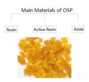
III Organic Solderability Preservative (OSP)
The general process is: degrease -> microetching -> pickling -> pure water cleaning -> organic coating -> cleaning. The process control is relatively easier than other indications.
OSP is a process for surface treatment of printed circuit board (PCB) copper foil in accordance with RoHS instructions.OSP is the abbreviation of Organic Solderability Preservatives. In a nutshell, OSP is a chemical process to grow a layer of organic skin on a clean bare copper surface.This film has anti-oxidation, heat shock and moisture resistance to protect copper surface from rust (oxidation or vulcanization, etc.) in normal environment.However, at subsequent welding temperatures, the protective film must be easily removed by the flux, so that the exposed clean copper surface can be immediately combined with the molten solder to form a solid solder spot in a very short time.
Advantages: simple process, smooth surface, suitable for lead-free soldering and SMT. Easy rework, convenient production operation, suitable for horizontal line operation. The board is suitable for multiple processing coexists (e.g. OSP+ENIG).Low cost and environmentally friendly.
Disadvantages: limited number of reflow soldering (multiple welding thickness, film will be damaged, basically two is fine). Not suitable for compression bonding, wire binding.Visual inspection and electrical testing are not convenient.N2 gas protection is required for SMT. SMT rework is not suitable.Storage conditions are high.
IV All-plate Nickel Plating
Nickel-gold plating is to coat the surface conductor of PCB with a layer of nickel and then a layer of gold. The main purpose of nickel plating is to prevent the diffusion between gold and copper.There are two types of electroplated nickel gold: soft gold (pure gold, with an unshiny surface) and hard gold (smooth and hard, wear-resistant, and containing other elements such as cobalt, with a shiny surface).Soft gold is mainly used for chip packaging with gold wire.Hard gold is mainly used for electrical interconnections in non-welds.
Advantages: longer storage time( more than 12 months); suitable for contact switch design and wire binding; suitable for electrical testing.
Disadvantages: higher cost, thicker gold. The electroplated finger requires additional design lines to conduct electricity. Due to the fact that the thickness of gold is not constant, it may lead to embrittlement and affect the strength when applied in welding. Problem of uniformity of electroplating surface. Electroplated nickel has no edge covering the wire. Not suitable for aluminum wire binding.
Nickel Plating
V Immersion Gold
The general process is: pickling cleaning -> microetching -> preleaching -> activation -> electroless nickel plating -> chemical leaching. There are 6 chemical tanks in the process, involving nearly 100 chemicals, and the process is relatively complex.
The immersion gold is a thick nickel gold alloy with good electrical properties on the copper surface, which can protect the PCB for a long time. It also has environmental tolerance that other surface treatment processes do not. Gold also prevents copper from dissolving, which would be beneficial for lead-free assembly.
Advantages: it is not easy to oxidize, and it can be stored for a long time, with smooth surface. It has the preferred option for a button PCB board (e.g., mobile phone board), and its reflow soldering can be repeated many times without reducing its solderability. It can be used as a base material for the COB (Chip On Board) line.
Immersion Gold Two-Layer PCB
VI Immersion Tin
Since all current solders are based on tin, so the tin layer can match any type of solder. The process of settling tin can form a flat copper-tin intergeneric compound, which makes it as weldable as hot air leveling without the flatness that is a headache.The solder plate cannot be stored for too long and must be assembled according to the order of the solder plate.
Advantages: suitable for horizontal production;suitable for refined line processing and lead-free welding, especially for compression welding; very good flatness, and suitable for SMT.
Disadvantages: requires good storage conditions, preferably no more than 6 months to control the growth of the tin whisker; not suitable for contact switch design; the production process has high requirements for the soldering film process, otherwise the soldering film will fall off ; it is best to use N2 gas when welding many times; electrical testing is also a problem.
Immersion Tin PCB
VII Immersion Silver
The silver precipitation process is between organic coating and chemical nickel plating/gold precipitation. Even when exposed to heat, moisture and pollution, silver remains well weldable, but it loses its luster. Sunken silver does not have the physical strength of electroless nickel/sunken gold because there is no nickel below the silver layer.
Advantages: simple process; suitable for lead-free soldering andSMT; very flat surface; low cost; suitable for very refined lines.
Disadvantages: high storage conditions and easy pollution; welding strength is prone to have problems (micro-cavity problems). It is easy to have the phenomenon of electromigration and the phenomenon of giovanni bite in the copper under the resistance welding film. Electrical testing is also a problem.
Immersion Silver PCB
VIII Chemical Nickel Palladium
Chemical nickel palladium is a layer of palladium between nickel and gold, which can prevent corrosion caused by replacement reaction and make full preparation for alloy deposit. Gold covers palladium tightly, providing a good interface.
Advantages: suitable for lead-free soldering. The surface is very flat and suitable for SMT. The through hole can also be plated with nickel gold. It has long storage time, and does not have harsh storage conditions. It’s suitable for electrical testing , for switch contact design, for aluminum wire binding, and for thick plate.
What is Palladium?
IX Electroplating Hard Gold
The purpose of electroplating hard gold is to improve the wear resistance of the product, increase the number of insertion and extraction and electroplating hard gold.
Changes in the surface treatment process of PCB are not great and seem to be a long way off, but it should be noted that slow changes over a long period of time will lead to great changes. PCB surface treatment technology is bound to change dramatically in the future as environmental concerns grow.
Hard Gold Plating PCB
You May Also Like:
Copying the Board, How Should I Copy It?
A Core Issue When Designing a PCB: Power-on
Structures and Applications of the FPCB
Ordering & Quality
| Photo | Mfr. Part # | Company | Description | Package | Qty |
|
MC33910G5AC | Company:NXP | Remark:IC SYSTEM BASIS CHIP 32LQFP | Package:32-LQFP |
MC33910G5AC Datasheet |
In Stock:5153 Inquiry |
Inquiry |
|
MC9S08QG8CPBE | Company:NXP / Freescale | Remark:IC MCU 8BIT 8KB FLASH 16DIP | Package:16-DIP (0.300", 7.62mm) |
MC9S08QG8CPBE Datasheet |
In Stock:5729 Inquiry |
Inquiry |

|
MC9S08QD4CSC | Company:NXP | Remark:IC MCU 8BIT 4KB FLASH 8SOIC | Package:SOIC8 |
MC9S08QD4CSC Datasheet |
In Stock:41393 Inquiry |
Inquiry |
|
MPC8280VVQLDA | Company:NXP / Freescale | Remark:IC MPU MPC82XX 333MHZ 408TBGA | Package:480-LBGA |
MPC8280VVQLDA Datasheet |
In Stock:744 Inquiry |
Inquiry |
|
K4S561632N-LC60 | Company:SAMSUNG | Remark:consumer memory | Package:TSOP |
K4S561632N-LC60 Datasheet |
In Stock:15960 Inquiry |
Inquiry |
|
MMB02070C2201FB200 | Company:VISHAY | Remark:RES SMD 2.2K OHM 1% 1W 0207 | Package:SMD |
MMB02070C2201FB200 Datasheet |
In Stock:63360 Inquiry |
Inquiry |
|
P87C554SBAA,512 | Company:NXP | Remark:IC MCU 8BIT 16KB OTP 68PLCC | Package:68-LCC (J-Lead) |
P87C554SBAA,512 Datasheet |
In Stock:510 Inquiry |
Inquiry |

|
LFE2-6SE-5FN256C | Company:Lattice Semiconductor | Remark:IC FPGA 190 I/O 256BGA | Package:256-BGA |
LFE2-6SE-5FN256C Datasheet |
In Stock:270 Inquiry |
Inquiry |
|
FC4L110R050FER | Company:Ohmite | Remark:RES SMD 0.05 OHM 5W 4320 WIDE | Package:Wide 4320 (11050 Metric), 2043 |
FC4L110R050FER Datasheet |
In Stock:481 Inquiry |
Inquiry |
|
DSS16-01AS | Company:IXYS | Remark:DIODE SCHOTTKY 100V 16A TO263AB | Package:TO-263-3, D²Pak (2 Leads + Tab), TO- |
DSS16-01AS Datasheet |
In Stock:580 Inquiry |
Inquiry |