| Manufacturer Part#: | XC7A200T-2FBG484I |
| Product Category: | Embedded - FPGAs (Field Programmable Gate Array) |
| Manufacturer: | Xilinx |
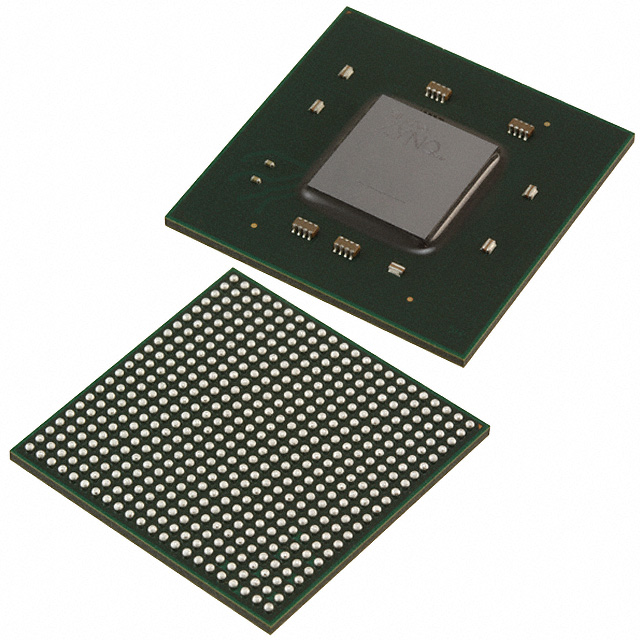
| Description: | IC FPGA ARTIX7 285 I/O 484FCBGA |
| Package: | BGA |
| Quantity: | 118 PCS |
| Lead Free Status / RoHS Status: | Lead free / RoHS Compliant |
| one to seven days | |
| Click buy button to purchase: | Buy |
CAD Models

XC7A200T-2FBG484I Symbol

XC7A200T-2FBG484I Footprint
Lifecycle Status Indicator

XC7A200T-2FBG484I Lifecycle Status Indicator
Product Attributes
Manufacturer | XILINX |
Category | Integrated Circuits (ICs) |
Family | Embedded - FPGAs (Field Programmable Gate Array) |
Series | Artix-7 |
Status | Active |
Brand | Xilinx |
Clock Management | MMCM, PLL |
Contact Plating | Copper, Tin, Silver |
Configuration Memory | 32MB QSPI |
REACH Compliant | Yes |
EU RoHS Compliant | Yes |
Device Logic Cells | 215360 |
Device Logic Units | 134600 |
Dedicated DSP | 740 |
Display Mode | HDMI Output; LCD Display (2 x 16) |
Ethernet | Yes |
GPIO | Yes |
Interface Standards | FMC HPC; I2C; Pmod; XADC; SMA; SFP |
JESD-30 Code | S-PBGA-B484 |
JESD-609 Code | e1 |
Mounting Type | Surface Mount |
Memory Card Interface | SD Card |
Memory Size | 1GB |
Memory Type | DDR3 |
Maximum Operating Temperature | 100 °C |
Minimum Operating Temperature | -40 °C |
Maximum Processing Temperature | 250 °C |
Maximum Operating Supply Voltage | 1.05 V |
Typical Operating Supply Voltage | 1 V |
Minimum Operating Supply Voltage | 0.95 V |
Maximum Clock Frequency | 1286 MHz |
Maximum Combinatorial Delay of a CLB | 1.05 ns |
Number of I/Os | 285 |
Number of Logic Blocks (LABs) | 16825 |
Number of Logic Elements/Cells | 215360 |
Number of Pins | 484 |
Number of Registers | 269200 |
Number of Inputs | 285 |
Number of Outputs | 285 |
Number of Multipliers | 740 (25x18) |
Device Number of DLLs/PLLs | 10 |
Total Number of Block RAM | 365 |
Organization | 16825 CLBS |
Package / Case | 484-BBGA, FCBGA |
Mfr Package Description | FBGA-484 |
Package Body Material | PLASTIC/EPOXY |
Package Code | BGA |
Package Equivalence Code | BGA484,22X22,40 |
Package Shape | SQUARE |
Package Style | GRID ARRAY |
Package Length | 23 mm |
Package Width | 23 mm |
Package Height | 1.84 mm |
Seated Plane Height | 2.34 mm |
Pin Pitch | 1 |
PCI Blocks | 1 |
Power Supplies | 1 V |
Process Technology | 28 nm |
Programmable Logic Type | FIELD PROGRAMMABLE GATE ARRAY |
Reflow Solder Time (Sec) | 30 |
Number of Reflow Cycle | 3 |
RAM Size | 13455360b |
Re-programmability Support | 1 |
Screening Level | Industrial |
Speed Grade | 2 |
Sub Category | Field Programmable Gate Arrays |
Supplier Device Package | 484-FCBGA (23x23) |
Technology | CMOS |
Terminal Finish | Tin/Silver/Copper (Sn/Ag/Cu) |
Terminal Form | BALL |
Terminal Position | BOTTOM |
Transceiver Blocks | 16 |
Transceiver Speed | 6.6Gbps |
USB | USB-Serial Bridge |
Features
● Advanced high-performance FPGA logic based on real 6-input lookup table (LUT) technology configurable as distributed memory.
● 36 Kb dual-port block RAM with built-in FIFO logic for on-chip data buffering.
● High-performance SelectIO™ technology with support for DDR3 interfaces up to 1,866 Mb/s.
● High-speed serial connectivity with built-in multi-gigabit transceivers from 600 Mb/s to maximum rates of 6.6 Gb/s up to 28.05 Gb/s, offering a special low-power mode, optimized for chip-to-chip interfaces.
● A user configurable analog interface (XADC), incorporating dual 12-bit 1MSPS analog-to-digital converters with on-chip thermal and supply sensors.
● DSP slices with 25 x 18 multiplier, 48-bit accumulator, and pre-adder for high-performance filtering, including optimized symmetric coefficient filtering.
● Powerful clock management tiles (CMT), combining phase-locked loop (PLL) and mixed-mode clock manager (MMCM) blocks for high precision and low jitter.
● Integrated block for PCI Express® (PCIe), for up to x8 Gen3 Endpoint and Root Port designs.
● Wide variety of configuration options, including support for commodity memories, 256-bit AES encryption with HMAC/SHA-256 authentication, and built-in SEU detection and correction.
● Low-cost, wire-bond, lidless flip-chip, and high signal integrity flipchip packaging offering easy migration between family members in the same package. All packages available in Pb-free and selected packages in Pb option.
● Designed for high performance and lowest power with 28 nm, HKMG, HPL process, 1.0V core voltage process technology and 0.9V core voltage option for even lower power.
Overview
Xilinx® 7 series FPGAs comprise three new FPGA families that address the complete range of system requirements, ranging from low cost, small form factor, cost-sensitive, high-volume applications to ultra high-end connectivity bandwidth, logic capacity, and signal processing capability for the most demanding high-performance applications. Artix®-7 Family: Optimized for lowest cost and power with small form-factor packaging for the highest volume applications.
Built on a state-of-the-art, high-performance, low-power (HPL), 28 nm, high-k metal gate (HKMG) process technology, 7 series FPGAs enable an unparalleled increase in system performance with 2.9 Tb/s of I/O bandwidth, 2 million logic cell capacity, and 5.3 TMAC/s DSP, while consuming 50% less power than previous generation devices to offer a fully programmable alternative to ASSPs and ASICs.
Advantages and Disadvantages
There is no relevant information available for this part yet.
Applications
There is no relevant information available for this part yet.
ECCN / UNSPSC
Description | Value |
ECCN | 3A991.d |
HTSN | PARTS... |
SCHEDULE B | PARTS... |
Documents & Media
Datasheets | |
PCN Design/Specification | |
PCN Assembly/Origin |
Product Manufacturer
Xilinx, Inc. is an American technology company, primarily a supplier of programmable logic devices. It is known as the semiconductor company that invented the field-programmable gate array (FPGA) and created the first fabless manufacturing model.
Ross Freeman, Bernard Vonderschmitt, and James V Barnett II, former employees of Zilog, an integrated circuit and solid-state device manufacturer, co-founded Xilinx in 1984 with headquarters in San Jose, USA.
Product Range
Devices | Boards | Developer Tools |
ACAPs | Accelerator Cards | Vivado Design Suite - HLx Editions |
FPGAs & 3D ICs | Evaluation Boards | SDAccel Development Environment |
SoCs, MPSoCs & RFSoCs
| System-on-Modules (SoMs) | SDSoC Development Environment |
Distributors
Distributors | Stock | Manufacturers | Descriptions |
Kynix | 118 | XILINX | IC FPGA ARTIX7 285 I/O 484FCBGA |
DigiKey | 348 | Xilinx Inc. | IC FPGA ARTIX7 285 I/O 484FCBGA |
Avnet | 0 | Xilinx | FPGA Artix-7 Family 215360 Cells 28nm Technology 1V 484-Pin Lidless FCBGA |
Farnell element14 | 0 | XILINX | FPGA ARTIX-7 285 I/O FCBGA-484 |
Chip One Exchange | 27 | XILINX | AVAILABLE ; DC: 2019+ |
Alternative Models
There is no relevant information available for this part yet.
Popularity by Region

XC7A200T-2FBG484I Popularity by Region
Market Price Analysis

XC7A200T-2FBG484I Market Price Analysis
Pictures


XC7A200T-2FBG484I Images
 IC FPGA 68 I/O 100VQFP
 IC FPGA 48 I/O 63WLCSP
 IC FPGA 500 I/O 900FCBGA