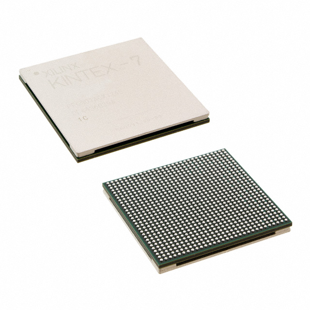
| Manufacturer Part#: | XC7K325T-2FFG900C |
| Product Category: | Embedded - FPGAs (Field Programmable Gate Array) |
| Manufacturer: | Xilinx |
| Description: | IC FPGA 500 I/O 900FCBGA |
| Package: | 900-BBGA, FCBGA |
| Quantity: | 1043 PCS |
| Lead Free Status / RoHS Status: | Lead free / RoHS Compliant |
| one to seven days | |
| Click buy button to purchase: | Buy |
CAD Models

XC7K325T-2FFG900C Symbol

XC7K325T-2FFG900C Footprint
Lifecycle Status Indicator

XC7K325T-2FFG900C Lifecycle Status Indicator
Product Attributes
Manufacturer | Xilinx Inc. |
Product Category | Embedded - FPGAs (Field Programmable Gate Array) |
Series | Kintex-7 |
status | Active |
Configuration Memory | 16MB QSPI; 128MB BPI FLASH |
Clock Management | MMCM, PLL |
Clock Frequency-Max | 1286.0 MHz |
Combinatorial Delay of a CLB-Max | 0.61 ns |
Dedicated DSP | 840 |
Device Logic Cells | 326,080 |
Device Logic Units | 203,800 |
Device Number of DLLs/PLLs | 10 |
Display Mode | HMDI Output |
REACH Compliant | Yes |
EU RoHS Compliant | Yes |
Interface Standards | FMC LPC; I2C; HPC; XADC; SMA; SFP+ |
JESD-30 Code | S-PBGA-B900 |
JESD-609 Code | e1 |
Lead Finish(Plating) | SnAgCu |
Mounting Type | Surface Mount |
Maximum Operating Temperature | 85 °C |
Minimum Operating Temperature | 0 °C |
Maximum Reflow Temperature | 245 °C |
Maximum Voltage Supply | 1.03 V |
Minimum Voltage Supply | 0.97 V |
Memory Card Interface | SD Card |
Memory Size | 1GB |
Memory Type | DDR3 |
Number of I/Os | 500 |
Number of Logic Blocks (LABs) | 25475 |
Number of Logic Elements/Cells | 326080 |
Total RAM Bits | 16404480 |
Total Number of Block RAM | 445 |
Number of Multipliers | 840 (25x18) |
Number of Registers | 407600 |
Number of Inputs | 500 |
Number of Outputs | 500 |
Number of Terminals | 900 |
Organization | 25475 CLBS |
Package / Case | 900-BBGA, FCBGA |
Mfr Package Description | FBGA-900 |
Package Body Material | PLASTIC/EPOXY |
Package Code | BGA |
Package Equivalence Code | BGA900,30X30,40 |
Package Shape | SQUARE |
Package Style | GRID ARRAY |
Power Supplies | 1,1.8,3.3 |
Pin Count | 900 |
PCI Blocks | 1 |
Process Technology | 28 nm |
Product Dimensions | 31 x 31 x 2.85 mm |
Length | 31.0 mm |
Width | 31.0 mm |
Height | 2.85 mm |
Programmable Logic Type | FIELD PROGRAMMABLE GATE ARRAY |
Program Memory Type | SRAM |
Re-programmability Support | 1 |
Reflow Solder Time (Sec) | 30 |
Screening Level | Commercial |
Seated Plane Height | 3.15 mm |
Speed Grade | -2 |
Sub Category | Field Programmable Gate Arrays |
Supplier Device Package | 900-FCBGA (31x31) |
Terminal Finish | Tin/Silver/Copper (Sn96.5Ag3.0Cu0.5) |
Terminal Form | BALL |
Terminal Pitch | 1 mm |
Terminal Position | BOTTOM |
Transceiver Blocks | 16 |
Transceiver Speed | 12.5 Gbps |
Typical Operating Supply Voltage | 1 V |
USB | USB-Serial Bridge |
Features
● Advanced high-performance FPGA logic based on real 6-input lookup table (LUT) technology configurable as distributed memory.
● 36 Kb dual-port block RAM with built-in FIFO logic for on-chip data buffering.
● High-performance SelectIO™ technology with support for DDR3 interfaces up to 1,866 Mb/s.
● High-speed serial connectivity with built-in multi-gigabit transceivers from 600 Mb/s to maximum rates of 6.6 Gb/s up to 28.05 Gb/s, offering a special low-power mode, optimized for chip-to-chip interfaces.
● A user configurable analog interface (XADC), incorporating dual 12-bit 1MSPS analog-to-digital converters with on-chip thermal and supply sensors.
● DSP slices with 25 x 18 multiplier, 48-bit accumulator, and pre-adder for high-performance filtering, including optimized symmetric coefficient filtering.
● Powerful clock management tiles (CMT), combining phase-locked loop (PLL) and mixed-mode clock manager (MMCM) blocks for high precision and low jitter.
● Integrated block for PCI Express® (PCIe), for up to x8 Gen3 Endpoint and Root Port designs.
● Wide variety of configuration options, including support for commodity memories, 256-bit AES encryption with HMAC/SHA-256 authentication, and built-in SEU detection and correction.
● Low-cost, wire-bond, lidless flip-chip, and high signal integrity flipchip packaging offering easy migration between family members in the same package. All packages available in Pb-free and selected packages in Pb option.
● Designed for high performance and lowest power with 28 nm, HKMG, HPL process, 1.0V core voltage process technology and 0.9V core voltage option for even lower power.
Overview
Xilinx® 7 series FPGAs comprise three new FPGA families that address the complete range of system requirements, ranging from low cost, small form factor, cost-sensitive, high-volume applications to ultra high-end connectivity bandwidth, logic capacity, and signal processing capability for the most demanding high-performance applications. Kintex®-7 Family: Optimized for best price-performance with a 2X improvement compared to previous generation, enabling a new class of FPGAs.
Built on a state-of-the-art, high-performance, low-power (HPL), 28 nm, high-k metal gate (HKMG) process technology, 7 series FPGAs enable an unparalleled increase in system performance with 2.9 Tb/s of I/O bandwidth, 2 million logic cell capacity, and 5.3 TMAC/s DSP, while consuming 50% less power than previous generation devices to offer a fully programmable alternative to ASSPs and ASICs.
Advantages and Disadvantages
There is no relevant information available for this part yet.
Applications
◆ Avionics for Kintex-7 FPGA
◆ LED Backlit Flat Panel Displays and 3DTV
◆ LTE Baseband Solution
ECCN / UNSPSC
Description | Value |
ECCN | 3A991D |
HTSN | 8542390001"8542.39.00.01 |
SCHEDULE B | 8542390000"8542.39.00.00 |
Documents & Media
Datsheets | |
PCN Design/Specification | |
PCN Assembly/Origin | |
Product Manufacturer
Xilinx, Inc.is an American technology company, primarily a supplier of programmable logic devices. It is known as the semiconductor company that invented the field-programmable gate array (FPGA) and created the first fabless manufacturing model.
Ross Freeman, Bernard Vonderschmitt, and James V Barnett II, former employees of Zilog, an integrated circuit and solid-state device manufacturer, co-founded Xilinx in 1984 with headquarters in San Jose, USA.
Product Range
Devices | Boards | Developer Tools |
ACAPs | Accelerator Cards | Vivado Design Suite - HLx Editions |
FPGAs & 3D ICs | Evaluation Boards | SDAccel Development Environment |
SoCs, MPSoCs & RFSoCs
| System-on-Modules (SoMs) | SDSoC Development Environment |
Distributors
Distributors | Stock | Manufacturers | Descriptions |
Kynix | 1043 | Xilinx Inc. | IC FPGA 500 I/O 900FCBGA |
DigiKey | 34 | Xilinx Inc. | IC FPGA 500 I/O 900FCBGA |
Avnet | 309 | Xilinx | FPGA Kintex-7 Family 326080 Cells 28nm Technology 1V 900-Pin FC-BGA |
Alternative Models
There is no relevant information available for this part yet.
Popularity by Region

XC7K325T-2FFG900C Popularity by Region
Market Price Analysis

XC7K325T-2FFG900C Market Price Analysis
Pictures


XC7K325T-2FFG900C Images
 IC FPGA 68 I/O 100VQFP
 IC FPGA 48 I/O 63WLCSP
 IC FPGA 60 I/O 81CSP