| Manufacturer Part#: | XC4VFX20-11FFG672I |
| Product Category: | Embedded - FPGAs (Field Programmable Gate Array) |
| Manufacturer: | Xilinx Inc. |
| Description: | IC FPGA 320 I/O 672FCBGA |
| Package: | 672-BBGA, FCBGA |
| Quantity: | 356 PCS |
| Lead Free Status / RoHS Status: | Lead free / RoHS Compliant |
| one to seven days | |
| Click buy button to purchase: | Buy |
CAD Models
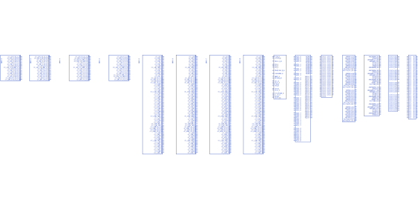
XC4VFX20-11FFG672I Symbol
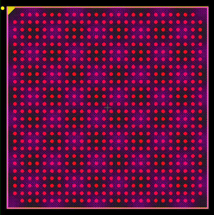
XC4VFX20-11FFG672I Footprint
Lifecycle Status Indicator
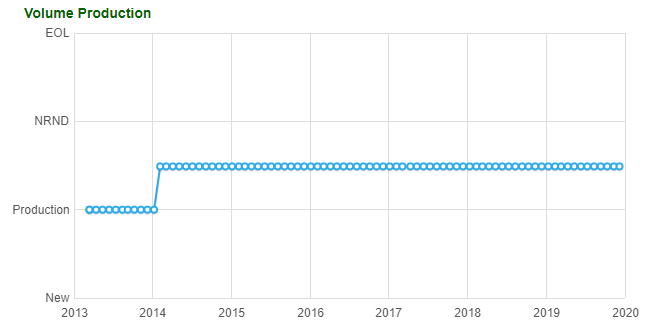
XC4VFX20-11FFG672I Lifecycle Status Indicator
Product Attributes
Categories | Integrated Circuits (ICs) Embedded - FPGAs (Field Programmable Gate Array) |
Manufacturer | Xilinx Inc. |
Series | Virtex®-4 FX |
Packaging | Tray |
Part Status | Active |
Number of LABs/CLBs | 2136 |
Number of Logic Elements/Cells | 19224 |
Total RAM Bits | 1253376 |
Number of I/O | 320 |
Voltage - Supply | 1.14V ~ 1.26V |
Mounting Type | Surface Mount |
Operating Temperature | -40°C ~ 100°C (TJ) |
Package / Case | 672-BBGA, FCBGA |
Supplier Device Package | 672-FCBGA (27x27) |
Base Part Number | XC4VFX20 |
Mfr Package Description | LEAD FREE, FBGA-672 |
REACH Compliant | Yes |
EU RoHS Compliant | Yes |
Status | Active |
Programmable Logic Type | FIELD PROGRAMMABLE GATE ARRAY |
Clock Frequency-Max | 1181.0 MHz |
JESD-30 Code | S-PBGA-B672 |
JESD-609 Code | e1 |
Moisture Sensitivity Level | 4 |
Number of CLBs | 2136.0 |
Number of Inputs | 320.0 |
Number of Logic Cells | 19224.0 |
Number of Outputs | 320.0 |
Number of Terminals | 672 |
Organization | 2136 CLBS |
Package Body Material | PLASTIC/EPOXY |
Package Code | BGA |
Package Equivalence Code | BGA672,26X26,40 |
Package Shape | SQUARE |
Package Style | GRID ARRAY |
Peak Reflow Temperature (Cel) | 245 |
Qualification Status | Not Qualified |
Seated Height-Max | 3.0 mm |
Sub Category | Field Programmable Gate Arrays |
Supply Voltage-Nom | 1.2 V |
Supply Voltage-Min | 1.14 V |
Supply Voltage-Max | 1.26 V |
Surface Mount | YES |
Technology | CMOS |
Terminal Finish | Tin/Silver/Copper (Sn95.5Ag4.0Cu0.5) |
Terminal Form | BALL |
Terminal Pitch | 1.0 mm |
Terminal Position | BOTTOM |
Time@Peak Reflow Temperature-Max (s) | 30 |
Length | 27.0 mm |
Width | 27.0 mm |
Overview
Combining Advanced Silicon Modular Block (ASMBL™) architecture with a wide variety of flexible features, the Virtex®-4 family from Xilinx greatly enhances programmable logic design capabilities, making it a powerful alternative to ASIC technology. Virtex-4 FPGAs comprise three platform families—LX, FX, and SX—offering multiple feature choices and combinations to address all complex applications. The wide array of Virtex-4 FPGA hard-IP core blocks includes the PowerPC® processors (with a new APU interface), tri-mode Ethernet MACs, 622 Mb/s to 6.5 Gb/s serial transceivers, dedicated DSP slices, high-speed clock management circuitry, and source-synchronous interface blocks. The basic Virtex-4 FPGA building blocks are enhancements of those found in the popular Virtex, Virtex-E, Virtex-II, Virtex-II Pro, and Virtex-II Pro X product families, so previous-generation designs are upward compatible. Virtex-4 devices are produced on a state-of-the-art 90 nm copper process using 300 mm (12-inch) wafer technology.
Features
Summary of Virtex-4 Family Features
• Three Families — LX/SX/FX
- Virtex-4 LX: High-performance logic applications solution
- Virtex-4 SX: High-performance solution for digital signal processing (DSP) applications
- Virtex-4 FX: High-performance, full-featured solution for embedded platform applications
• Xesium™ Clock Technology
- Digital clock manager (DCM) blocks
- Additional phase-matched clock dividers (PMCD)
- Differential global clocks
• XtremeDSP™ Slice
- 18 x 18, two’s complement, signed Multiplier
- Optional pipeline stages
- Built-in Accumulator (48-bit) and Adder/Subtracter
• Smart RAM Memory Hierarchy
- Distributed RAM
- Dual-port 18-Kbit RAM blocks
· Optional pipeline stages
· Optional programmable FIFO logic automatically remaps RAM signals as FIFO signals
- High-speed memory interface supports DDR and DDR-2 SDRAM, QDR-II, and RLDRAM-II.
• SelectIO™ Technology
- 1.5V to 3.3V I/O operation
- Built-in ChipSync™ source-synchronous technology
- Digitally controlled impedance (DCI) active termination
- Fine grained I/O banking (configuration in one bank)
• Flexible Logic Resources
• Secure Chip AES Bitstream Encryption
• 90 nm Copper CMOS Process
• 1.2V Core Voltage
• Flip-Chip Packaging including Pb-Free Package Choices
• RocketIO™ 622 Mb/s to 6.5 Gb/s Multi-Gigabit Transceiver (MGT) [FX only]
• IBM PowerPC RISC Processor Core [FX only]
- PowerPC 405 (PPC405) Core
- Auxiliary Processor Unit Interface (User Coprocessor)
• Multiple Tri-Mode Ethernet MACs [FX only]
Advantages and Disadvantages
There is no relevant information available for this part yet.
Applications
There is no relevant information available for this part yet.
Compliance
RoHS | Compliant |
Radiation Hardening | No |
REACH SVHC | No SVHC |
ECCN / UNSPSC
Description | Value |
ECCN | 3A991.D |
HTSN | 8542390001 |
SCHEDULE B | 8542390000 |
Documents & Media
Datasheets | |
Design Resources |
Product Manufacturer
Xilinx, Inc. is an American technology company and is primarily a supplier of programmable logic devices. It is known for inventing the field-programming gate array and as the semiconductor company that created the first fabless manufacturing model. Ross Freeman, Bernard Vonderschmitt, and James V Barnett II, former employees of Zilog, an integrated circuit and solid-state device manufacturer, co-founded Xilinx in 1984 with headquarters in San Jose, USA.
Product Range
Devices | Boards | Developer Tools |
ACAPs | Accelerator Cards | Vivado Design Suite - HLx Editions |
FPGAs & 3D ICs | Evaluation Boards | SDAccel Development Environment |
SoCs, MPSoCs & RFSoCs | System-on-Modules (SoMs) | SDSoC Development Environment |
Distributors
Distributors | Stock | Manufacturers | Descriptions |
Kynix | 356 PCS | Xilinx Inc. | IC FPGA 320 I/O 672FCBGA |
DigiKey | Non-stock | Xilinx Inc. | IC FPGA 320 I/O 672FCBGA |
Mouser | 6 PCS | Xilinx | FPGA - Field Programmable Gate Array Connect to S1 BOM Open O/E MH = Yes make quotable per DJ |
Alternative Models
There is no relevant information available for this part yet.
Popularity by Region
There is no relevant information available for this part yet.
Market Price Analysis
XC4VFX20-11FFG672I Market Price Analysis
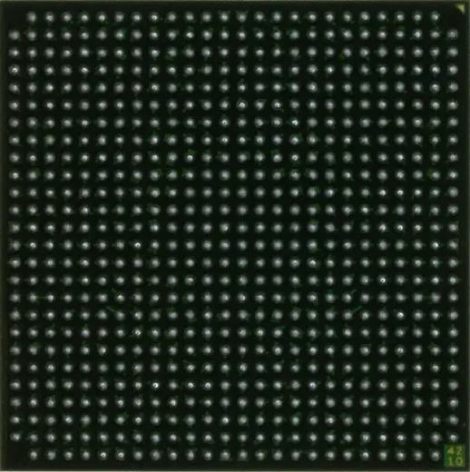
Pictures
XC4VFX20-11FFG672I Images
 IC FPGA 68 I/O 100VQFP
 IC FPGA 48 I/O 63WLCSP
 IC FPGA 500 I/O 900FCBGA