| Manufacturer Part#: | XC6VLX130T-L1FFG1156I |
| Product Category: | Embedded - FPGAs (Field Programmable Gate Array) |
| Manufacturer: | Xilinx Inc. |
| Description: | IC FPGA 600 I/O 1156FCBGA |
| Package: | 1156-BBGA, FCBGA |
| Quantity: | 146 PCS |
| Lead Free Status / RoHS Status: | Lead free / RoHS Compliant |
| one to seven days | |
| Click buy button to purchase: | Buy |
CAD Models
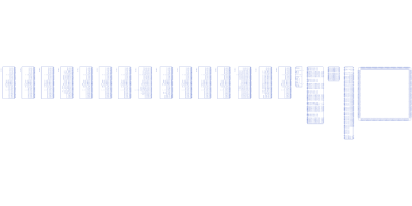
XC6VLX130T-L1FFG1156I Symbol
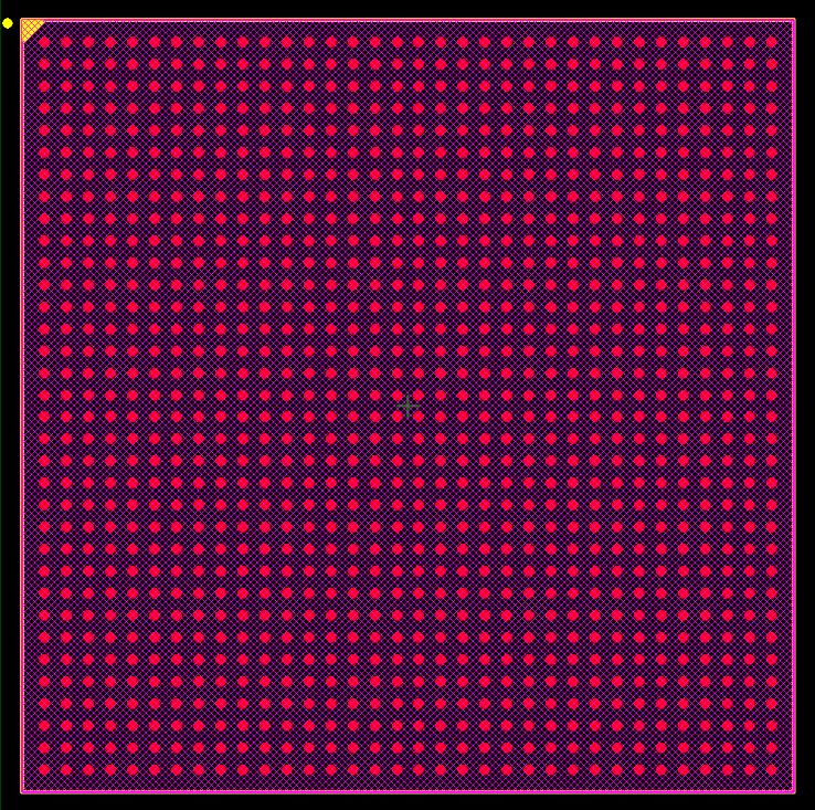
XC6VLX130T-L1FFG1156I Footprint
Lifecycle Status Indicator
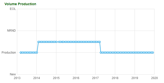
XC6VLX130T-L1FFG1156I Lifecycle Status Indicator
Product Attributes
Categories | Integrated Circuits (ICs) Embedded - FPGAs (Field Programmable Gate Array) |
Manufacturer | Xilinx Inc. |
Series | Virtex®-6 LXT |
Packaging | Tray |
Part Status | Active |
Number of LABs/CLBs | 10000 |
Number of Logic Elements/Cells | 128000 |
Total RAM Bits | 9732096 |
Number of I/O | 600 |
Voltage - Supply | 0.91V ~ 0.97V |
Mounting Type | Surface Mount |
Operating Temperature | -40°C ~ 100°C (TJ) |
Package / Case | 1156-BBGA, FCBGA |
Supplier Device Package | 1156-FCBGA (35x35) |
Base Part Number | XC6VLX130T |
Mfr Package Description | 35 X 35 MM, LEAD FREE, FBGA-1156 |
REACH Compliant | Yes |
EU RoHS Compliant | Yes |
Status | Active |
Programmable Logic Type | FIELD PROGRAMMABLE GATE ARRAY |
Clock Frequency-Max | 1098.0 MHz |
Combinatorial Delay of a CLB-Max | 5.87 ns |
JESD-30 Code | S-PBGA-B1156 |
JESD-609 Code | e1 |
Moisture Sensitivity Level | 4 |
Number of Inputs | 600.0 |
Number of Logic Cells | 128000.0 |
Number of Outputs | 600.0 |
Number of Terminals | 1156 |
Operating Temperature-Min | -40.0 Cel |
Operating Temperature-Max | 100.0 Cel |
Package Body Material | PLASTIC/EPOXY |
Package Code | BGA |
Package Equivalence Code | BGA1156,34X34,40 |
Package Shape | SQUARE |
Package Style | GRID ARRAY |
Peak Reflow Temperature (Cel) | 245 |
Power Supplies | 1,1.2/2.5 |
Qualification Status | Not Qualified |
Seated Height-Max | 3.5 mm |
Sub Category | Field Programmable Gate Arrays |
Supply Voltage-Nom | 0.9 V |
Supply Voltage-Min | 0.87 V |
Supply Voltage-Max | 0.93 V |
Surface Mount | YES |
Technology | CMOS |
Temperature Grade | INDUSTRIAL |
Terminal Finish | Tin/Silver/Copper (Sn96.5Ag3.0Cu0.5) |
Terminal Form | BALL |
Terminal Pitch | 1.0 mm |
Terminal Position | BOTTOM |
Time@Peak Reflow Temperature-Max (s) | 30 |
Length | 35.0 mm |
Width | 35.0 mm |
Overview
Virtex®-6 FPGAs are the programmable silicon foundation for Targeted Design Platforms that deliver integrated software and hardware components to enable designers to focus on innovation as soon as their development cycle begins. Using the third-generation ASMBL™ (Advanced Silicon Modular Block) column-based architecture, the Virtex-6 family contains multiple distinct sub-families. This overview covers the devices in the LXT, SXT, and HXT sub-families. Each sub-family contains a different ratio of features to most efficiently address the needs of a wide variety of advanced logic designs. In addition to the high-performance logic fabric, Virtex-6 FPGAs contain many builtin system-level blocks. These features allow logic designers to build the highest levels of performance and functionality into their FPGAbased systems. Built on a 40 nm state-of-the-art copper process technology, Virtex-6 FPGAs are a programmable alternative to custom ASIC technology. Virtex-6 FPGAs offer the best solution for addressing the needs of high-performance logic designers, high-performance DSP designers, and high-performance embedded systems designers with unprecedented logic, DSP, connectivity, and soft microprocessor capabilities.
Features
·Three sub-families:
• Virtex-6 LXT FPGAs: High-performance logic with advanced serial connectivity
• Virtex-6 SXT FPGAs: Highest signal processing capability with advanced serial connectivity
• Virtex-6 HXT FPGAs: Highest bandwidth serial connectivity
·Compatibility across sub-families
• LXT and SXT devices are footprint compatible in the same package
·Advanced, high-performance FPGA Logic
• Real 6-input look-up table (LUT) technology
• Dual LUT5 (5-input LUT) option
• LUT/dual flip-flop pair for applications requiring rich register mix
• Improved routing efficiency
• 64-bit (or two 32-bit) distributed LUT RAM option per 6-input LUT
• SRL32/dual SRL16 with registered outputs option
·Powerful mixed-mode clock managers (MMCM)
• MMCM blocks provide zero-delay buffering, frequency synthesis, clock-phase shifting, inputjitter filtering, and phase-matched clock division
·36-Kb block RAM/FIFOs
• Dual-port RAM blocks
• Programmable
- Dual-port widths up to 36 bits
- Simple dual-port widths up to 72 bits
• Enhanced programmable FIFO logic
• Built-in optional error-correction circuitry
• Optionally use each block as two independent 18 Kb blocks
·High-performance parallel SelectIO™ technology
• 1.2 to 2.5V I/O operation
• Source-synchronous interfacing using ChipSync™ technology
• Digitally controlled impedance (DCI) active termination
• Flexible fine-grained I/O banking
• High-speed memory interface support with integrated write-leveling capability
·Advanced DSP48E1 slices
• 25 x 18, two's complement multiplier/accumulator
• Optional pipelining
• New optional pre-adder to assist filtering applications
• Optional bitwise logic functionality
• Dedicated cascade connections
·Flexible configuration options
• SPI and Parallel Flash interface
• Multi-bitstream support with dedicated fallback reconfiguration logic
• Automatic bus width detection
·System Monitor capability on all devices
• On-chip/off-chip thermal and supply voltage monitoring
• JTAG access to all monitored quantities
·Integrated interface blocks for PCI Express® designs
• Compliant to the PCI Express Base Specification 2.0
• Gen1 (2.5 Gb/s) and Gen2 (5 Gb/s) support with GTX transceivers
• Endpoint and Root Port capable
• x1, x2, x4, or x8 lane support per block
·GTX transceivers: up to 6.6 Gb/s
• Data rates below 480 Mb/s supported by oversampling in FPGA logic.
·GTH transceivers: 2.488 Gb/s to beyond 11 Gb/s
·Integrated 10/100/1000 Mb/s Ethernet MAC block
• Supports 1000BASE-X PCS/PMA and SGMII using GTX transceivers
• Supports MII, GMII, and RGMII using SelectIO technology resources
• 2500Mb/s support available
·40 nm copper CMOS process technology
·1.0V core voltage (-1, -2, -3 speed grades only)
·Lower-power 0.9V core voltage option (-1L speed grade only)
·High signal-integrity flip-chip packaging available in standard or Pb-free package options
Advantages and Disadvantages
There is no relevant information available for this part yet.
Applications
There is no relevant information available for this part yet.
Compliance
RoHS | Compliant |
Radiation Hardening | No |
REACH SVHC | No SVHC |
ECCN / UNSPSC
Description | Value |
ECCN | 3A991D |
HTSN | 8542.39.00.01 |
SCHEDULE B | 8542.39.00.00 |
Documents & Media
Datasheets | |
Product Training Modules | |
Design Resources | |
PCN Design/Specification | Virtex-6 FIFO Input Logic Reset 18/Apr/2011 |
PCN Assembly/Origin | |
HTML Datasheet |
Product Manufacturer
Xilinx, Inc. is an American technology company and is primarily a supplier of programmable logic devices. It is known for inventing the field-programming gate array and as the semiconductor company that created the first fabless manufacturing model. Ross Freeman, Bernard Vonderschmitt, and James V Barnett II, former employees of Zilog, an integrated circuit and solid-state device manufacturer, co-founded Xilinx in 1984 with headquarters in San Jose, USA.
Product Range
Devices | Boards | Developer Tools |
ACAPs | Accelerator Cards | Vivado Design Suite - HLx Editions |
FPGAs & 3D ICs | Evaluation Boards | SDAccel Development Environment |
SoCs, MPSoCs & RFSoCs | System-on-Modules (SoMs) | SDSoC Development Environment |
Distributors
Distributors | Stock | Manufacturers | Descriptions |
Kynix | 146 PCS | Xilinx Inc. | IC FPGA 600 I/O 1156FCBGA |
DigiKey | Non-Stock | Xilinx Inc. | IC FPGA 600 I/O 1156FCBGA |
Mouser | Non-Stock | Xilinx | FPGA - Field Programmable Gate Array XC6VLX130T-L1FFG1156I |
Alternative Models
There is no relevant information available for this part yet.
Popularity by Region
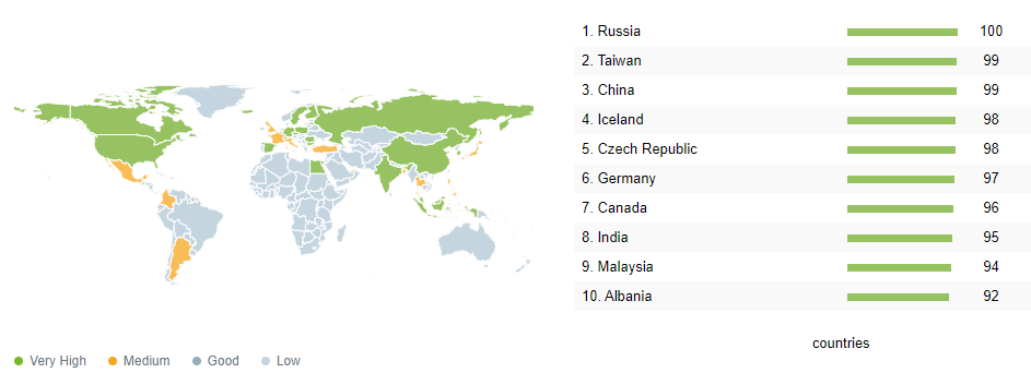
XC6VLX130T-L1FFG1156I Popularity by Region
Market Price Analysis
There is no relevant information available for this part yet.
Pictures

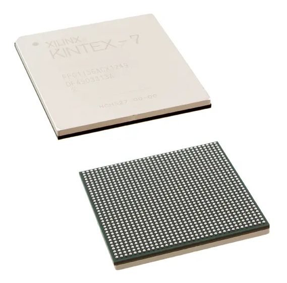
XC6VLX130T-L1FFG1156I Images
 IC FPGA 68 I/O 100VQFP
 IC FPGA 48 I/O 63WLCSP
 IC FPGA 500 I/O 900FCBGA