7
Catalog
I Introduction | |
II Interference Coupling Method | 2.1 Conductive EMI |
2.2 Common Impedance Coupling | |
2.3 Radiation Coupling | |
2.4 Radiation Emission | |
III Factors Affecting EMC | 3.1 Voltage |
3.2 Frequency | |
3.3 Ground | |
3.4 PCB design | |
3.5 Power supply decoupling | |
IV Electromagnetic Compatibility Design of PCB | 3.1 General principles of PCB design |
3.2 PCB and circuit anti-interference measures | |
I Introduction
As single-chip systems are more and more widely used in consumer electronics, medical, industrial automation, intelligent instrumentation, aerospace and other fields, single-chip systems are facing increasing threats of electromagnetic interference (EMI). Electromagnetic compatibility (EMC) covers both the emission and sensitivity of the system. If a microcontroller system meets the following three conditions, the system is electromagnetically compatible:
(1) It does not cause interference to other systems;
(2) It's not sensitive to the transmission of other systems;
(3) No interference to the system itself.
If the interference cannot be completely eliminated, but also to minimize interference. The generation of interference is either direct (via conductors, common impedance coupling, etc.) or indirect (by crosstalk or radiative coupling). Electromagnetic interference is generated by conductors and by radiation. Many electromagnetic sources such as light, relays, DC motors and fluorescent lamps can cause interference. The internal circuits of AC power lines, interconnecting cables, metal cables and subsystems can also generate radiation. Or receive an unwanted signal. In high-speed microcontroller systems, clock circuits are often the largest source of broadband noise, which can generate harmonic distortions of up to 300 MHz, which should be removed in the system. In addition, in the microcontroller system, the most susceptible are the reset line, the interrupt line and the control line.
II Interference Coupling Method
2.1 Conductive EMI
One of the most obvious and often overlooked paths that cause noise in the circuit is through the conductor. A wire that passes through a noisy environment picks up noise and sends it to other circuits to cause interference. Designers must avoid wire pick-up noise and decoupling to remove noise before noise causes interference. The most common example is noise entering the circuit through the power line. If the power supply itself or other circuitry connected to the power supply is the source of interference, the power supply must be decoupled before it enters the circuit.
2.2 Common Impedance Coupling
Co-impedance coupling occurs when current from two different circuits flows through a common impedance. The voltage drop across the impedance is determined by two circuits, and the ground current from the two circuits flows through the common ground impedance. The ground potential of circuit 1 is modulated by ground current 2, and a noise signal or DC compensation is coupled from circuit 2 to circuit 1 via a common ground impedance.
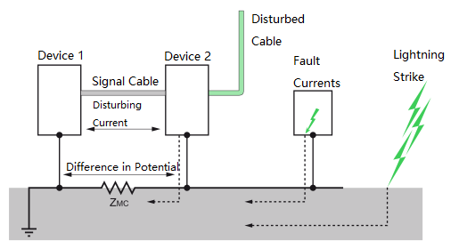
Example of Common-mode Impedance Coupling
2.3 Radiation Coupling
The coupled radiation is known as crosstalk. Crosstalk occurs when an electric current flows through a conductor to generate an electromagnetic field that induces a transient current in an adjacent conductor.
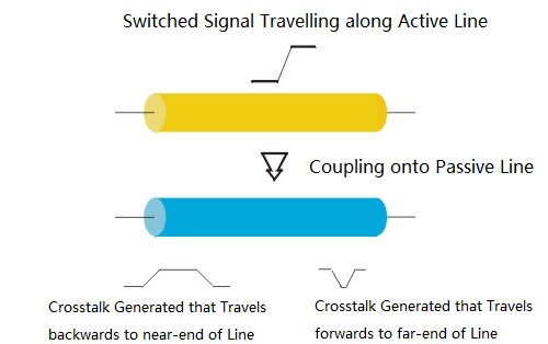
Overview of Crosstalk Induced Noise
2.4 Radiation Emission
There are two basic types of radiated emissions: differential mode (DM) and common mode (CM). Common mode radiation or monopole antenna radiation is caused by an unintentional voltage drop that raises all ground connections in the circuit above the system ground potential. In terms of electric field size, CM radiation is a more serious problem than DM radiation. To minimize CM radiation, the common mode current must be reduced to zero with a realistic design.
III Factors Affecting EMC
3.1 Voltage
The higher the supply voltage, the greater the voltage amplitude and the higher the emissions, while the lower supply voltage affects the sensitivity.
3.2 Frequency
High frequencies produce more emissions, and periodic signals produce more emissions. In a high-frequency single-chip system, a current spike is generated when the device is switched; in an analog system, a current spike is generated when the load current changes.
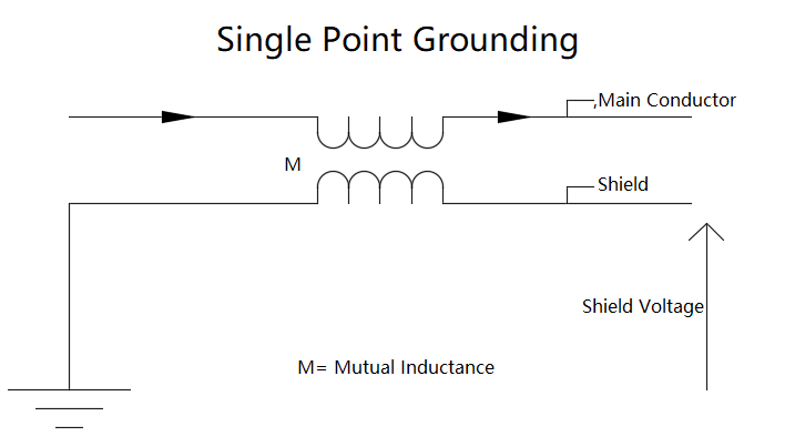
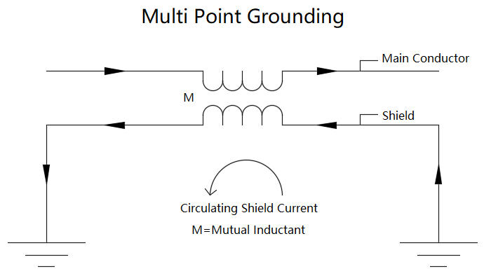
3.3 Ground
Among all EMC issues, the main problem is caused by improper grounding. There are three methods of signal grounding: single point, multiple points, and hybrid. At frequencies below 1 MHz, a single point grounding method can be used, but not for high frequencies; in high frequency applications, multipoint grounding is preferred. Hybrid grounding is a method in which the low frequency is grounded at a single point and the high frequency is grounded at multiple points. The ground layout is the key, and the ground loop of the high-frequency digital circuit and the low-level analog circuit must not be mixed.
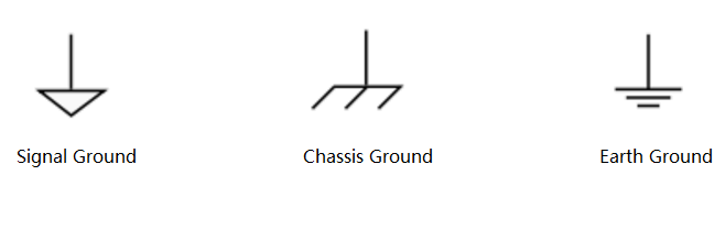
Grounding Symbols
3.4 PCB Design
Proper printed circuit board (PCB) wiring is critical to preventing EMI.
3.5 Power Supply Decoupling
When the device is switched, transient currents are generated on the power line and these transient currents must be attenuated and filtered out. Transient currents from high di/dt sources cause ground and trace "emission" voltages, high di/dt produces a wide range of high frequency currents, excitation components and cable radiation. Current changes and inductance through the wire can cause a voltage drop that can be minimized by reducing inductance or current changes over time.
IV Electromagnetic Compatibility Design of PCB
A PCB is a support for circuit components and devices in a microcontroller system that provides electrical connections between circuit components and devices. With the rapid development of electronic technology, the density of PCBs is getting higher and higher. The quality of PCB design has a great influence on the electromagnetic compatibility of single-chip microcomputer system. Practice has proved that even if the circuit schematic design is correct and the printed circuit board is not properly designed, it will have an adverse effect on the reliability of the single-chip system. For example, if the two thin parallel lines of the printed board are in close proximity, a delay in the signal waveform is formed, and reflected noise is formed at the end of the transmission line. Therefore, when designing a printed circuit board, care should be taken to adopt the correct method, to comply with the general principles of PCB design, and to comply with the requirements of anti-interference design.
3.1 General Principles of PCB Design
In order to get the best performance of the electronic circuit, the layout of the components and the layout of the wires are very important. In order to design a good quality, low cost PCB, the following general principles should be followed.
(1) Special Component Layout
First, consider the size of the PCB: when the PCB size is too large, the printed lines are long, the impedance is increased, the anti-noise ability is reduced, and the cost is also increased; if it is too small, the heat dissipation is not good, and the adjacent lines are susceptible to interference. After determining the PCB size, determine the location of the special components. Finally, according to the functional unit of the circuit, all the components of the circuit are laid out.
Observe the following principles when determining the location of a particular component:
1) Minimize the wiring between high-frequency components and try to reduce their distribution parameters and mutual electromagnetic interference. Components that are susceptible to interference cannot be placed too close together, and input and output components should be kept as far away as possible.
2) There may be a high potential difference between some components or wires. The distance between them should be increased to avoid accidental short circuit caused by discharge. Components with high voltage should be placed as far as possible in the hands of the hand when debugging.
3) Components weighing more than 15g should be fixed with brackets and then soldered. Those components that are large, heavy, and have a lot of heat should not be mounted on the printed board, but should be installed on the chassis of the whole machine, and heat dissipation should be considered. The thermal element should be kept away from the heating element.
4) For the layout of adjustable components such as potentiometers, adjustable inductors, variable capacitors, and microswitches, the structural requirements of the complete machine should be considered. If it is adjusted inside the machine, it should be placed on the printing plate for easy adjustment; if it is adjusted outside the machine, its position should be adapted to the position of the adjustment knob on the chassis panel.
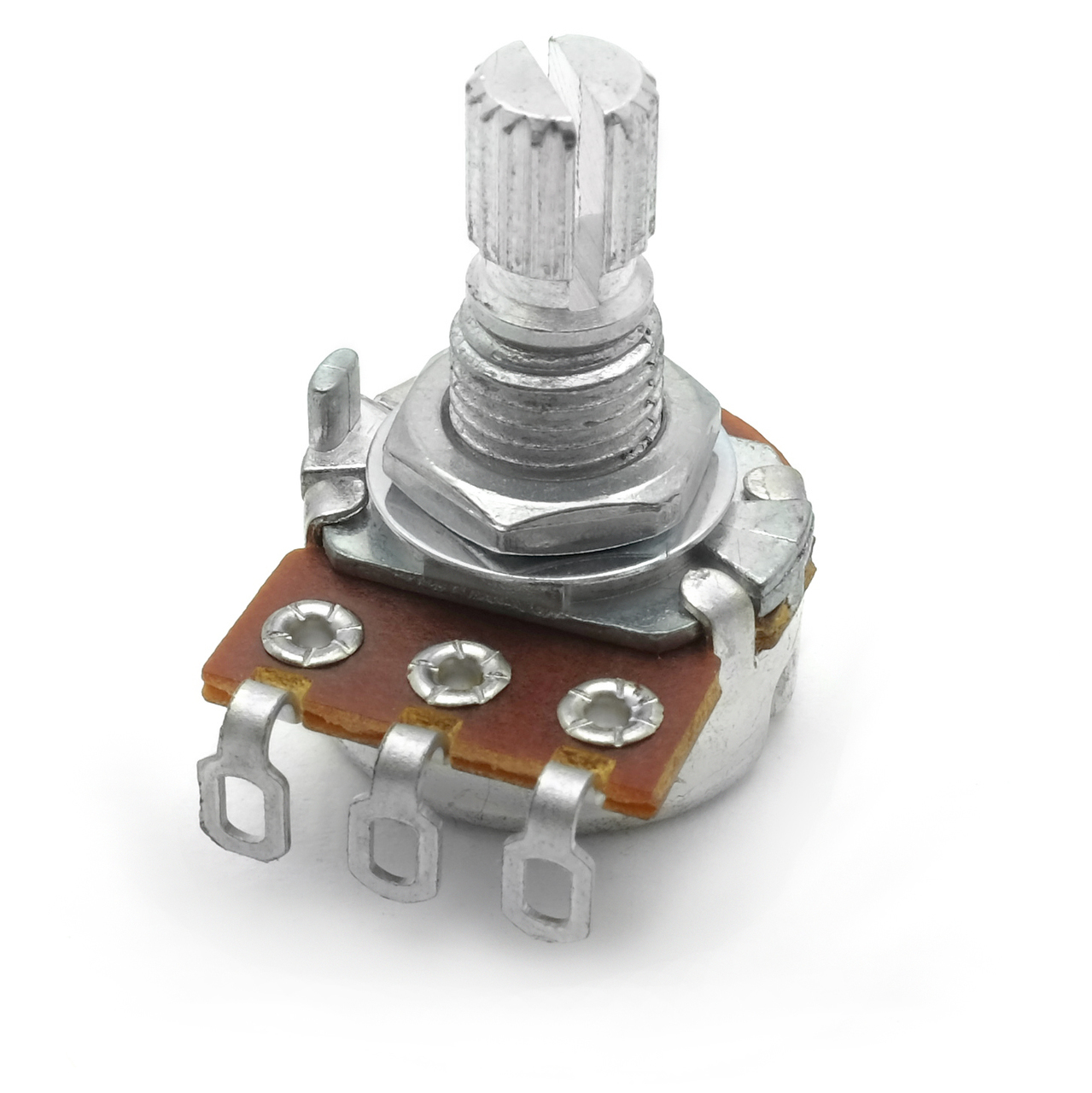
A Common Potentiometer
5) Leave the position occupied by the positioning holes of the printing plate and the fixing bracket.
(2) General Component Layout
According to the functional unit of the circuit, when laying out all the components of the circuit, the following principles must be met:
1) Arrange the position of each functional circuit unit according to the flow of the circuit, so that the layout facilitates signal circulation and keeps the signal as consistent as possible.
2) Center around the core components of each functional circuit and arrange it around it. Components should be evenly, neatly and compactly arranged on the PCB to minimize and shorten leads and connections between components.
3) For circuits operating at high frequencies, consider the distribution parameters between components. Generally, the circuit should be arranged in parallel as much as possible, so that it is not only beautiful, but also easy to load and weld, and easy to mass-produce.
4) Components located at the edge of the board are typically no less than 2 mm from the edge of the board. The optimal shape of the board is a rectangle. The aspect ratio is 3:2 or 4:3. When the board surface size is larger than 200 mm × 150 mm, the mechanical strength of the board should be considered.
(3) Principles of Wiring are as Follows:
1) The wires used for the input and output terminals should be avoided as far as possible, and it is better to add the ground wire between the wires to avoid feedback coupling.
2) The minimum width of the printed board wires is mainly determined by the adhesion strength between the wires and the insulating substrate and the current flowing through them. When the thickness of the copper foil is 0.5 mm and the width is 1 to 15 mm, the temperature rise is not higher than 3 °C by the current of 2 A. Therefore, a wire width of 1.5 mm is sufficient. For integrated circuits, especially digital circuits, a wire width of 0.02 to 0.3 mm is usually selected. Of course, as far as possible, use wide lines, especially power and ground. The minimum spacing of the wires is primarily determined by the worst case interline insulation resistance and breakdown voltage. For integrated circuits, especially digital circuits, the pitch can be less than 0.1 to 0.2 mm as long as the process allows.
3) The curved corner of the printed wire generally takes a circular arc shape, and the right angle or angle affects the electrical performance in the high frequency circuit. In addition, try to avoid the use of large-area copper foil, otherwise, when heated for a long time, copper foil expansion and falling off are prone to occur. When a large area of copper foil is used, it is preferable to use a grid shape, which is advantageous for eliminating the volatile gas generated by the heat of the adhesive between the copper foil and the substrate.
4) The center hole of the pad is slightly larger than the diameter of the device lead. The pad is too large to form a solder joint. The pad outer diameter D is generally not less than (d + 1.2) mm, where d is the lead aperture. For high-density digital circuits, the minimum pad diameter can be (d + 1.0) mm.
3.2 PCB and Circuit Anti-interference Measures
The anti-jamming design of printed circuit boards is closely related to the specific circuit. Here, only some common measures of PCB anti-interference design are explained.
(1) Power Cord Design
According to the current of the printed circuit board, the power line width should be increased as much as possible to reduce the loop resistance. At the same time, the direction of the power line and the ground line and the direction of data transmission are the same, which helps to enhance the anti-noise capability.
(2) Ground Design
In the design of single chip microcomputer system, grounding is an important method to control interference. If the grounding and shielding are properly combined, most of the interference problems can be solved. The ground wire structure in the single chip microcomputer system is roughly systematic, chassis ground (shielded ground), digital ground (logical ground) and analog ground. Pay attention to the following points in the ground line design:
1) Correctly select single point grounding and multi-point grounding. In the low-frequency circuit, the operating frequency of the signal is less than 1 MHz, and the influence of the inductance between the wiring and the device is small, and the circulating current formed by the grounding circuit has a great influence on the interference, so a grounding method should be adopted. When the signal operating frequency is greater than 10 MHz, the ground impedance becomes very large. In this case, the ground impedance should be reduced as much as possible. When the operating frequency is between 1 and 10 MHz, if a grounding is used, the grounding length should not exceed 1/20 of the wavelength. Otherwise, the multi-point grounding method should be used.
2) Digital ground is separated from analog ground. The circuit board has both high-speed logic circuits and linear circuits. They should be separated as much as possible, and the ground wires of the two should not be mixed, and they are connected to the power ground. The ground of the low-frequency circuit should be grounded in parallel at a single point. When the actual wiring is difficult, it can be partially connected and then connected in parallel. The high-frequency circuit should be connected in series with multiple points. The ground wire should be short and thick. Try to use a grid-like large-area foil around the high-frequency components, and try to increase the grounding area of the linear circuit.
Linear Circuit
3) Digital ground is separated from analog ground. The circuit board has both high-speed logic circuits and linear circuits. They should be separated as much as possible, and the ground wires of the two should not be mixed, and they are connected to the power ground. The ground of the low-frequency circuit should be grounded in parallel at a single point. When the actual wiring is difficult, it can be partially connected and then connected in parallel. The high-frequency circuit should be connected in series with multiple points. The ground wire should be short and thick. Try to use a grid-like large-area foil around the high-frequency components, and try to increase the grounding area of the linear circuit.
4) The ground wire forms a closed loop. When designing a grounding system for a printed circuit board consisting only of digital circuits, making the grounding wire closed can significantly improve the noise immunity. The reason is that there are many integrated circuit components on the printed circuit board, especially when there are many power-consuming components, due to the limitation of the grounding wire thickness, a large potential difference will be generated on the ground wire, causing the noise resistance to decrease; If the ground line is formed into a loop, the potential difference is reduced, and the noise resistance of the electronic device is improved.
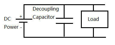
(3) Decoupling Capacitor Configuration
One of the usual practices in PCB design is to configure the appropriate decoupling capacitors at each critical part of the printed board. The general configuration principle for decoupling capacitors is:
1) The power input terminal is connected to an electrolytic capacitor of 10 to 100 μF. If possible, it is better to connect 100μF or more.
2) In principle, a 0.01 pF ceramic capacitor should be placed on each integrated circuit chip. If the printed board gap is not enough, a 1~10 pF tantalum capacitor can be placed every 4~8 chips.
3) For devices with weak anti-noise capability and large power supply changes during shutdown, such as RAM and ROM memory devices, decoupling capacitors should be directly connected between the power and ground lines of the chip.
4) The capacitor leads should not be too long, especially the high-frequency bypass capacitors must not have leads.
In addition, you should also pay attention to the following two points:
1) When there are contactors, relays, buttons and other components in the printed board, a large spark discharge will occur when operating them, and an RC circuit must be used to absorb the discharge current. Generally, R takes 1 to 2 kΩ, and C takes 2.2 to 47 μF.
2) CMOS input impedance is very high, and it is susceptible to induction, so when it is used, it should be grounded or connected to the power supply.
Capacitor Placed in Parallel for Decoupling
(4) Oscillator
Almost all microcontrollers have an oscillator circuit that is coupled to an external crystal or ceramic resonator. On the PCB, the lead of the external capacitor, crystal or ceramic resonator is required to be as short as possible. The RC oscillator is potentially sensitive to interfering signals, it can produce very short clock cycles, so it is best to choose a crystal or ceramic resonator. In addition, the outer casing of the quartz crystal should be grounded.
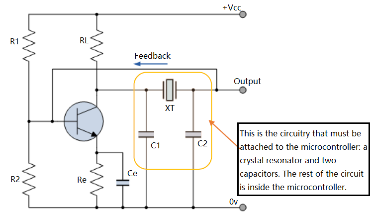
Crystal Oscillator Circuit
(5) Lightning Protection Measures
The outdoor-use single-chip microcomputer system or the power line and signal line that is introduced into the room from the outdoor overhead should consider the lightning protection problem of the system. Commonly used lightning protection devices are: gas discharge tube, TVS (Transient Voltage Suppression) and the like. The gas discharge tube is a gas breakdown discharge when the power supply voltage is greater than a certain value, usually tens of V or hundreds of V, and the strong shock pulse on the power line is introduced into the earth. The TVS can be viewed as two parallel and opposite-direction Zener diodes that conduct when the voltage across the terminals is above a certain value. It is characterized by the ability to transiently pass hundreds or even thousands of A currents.
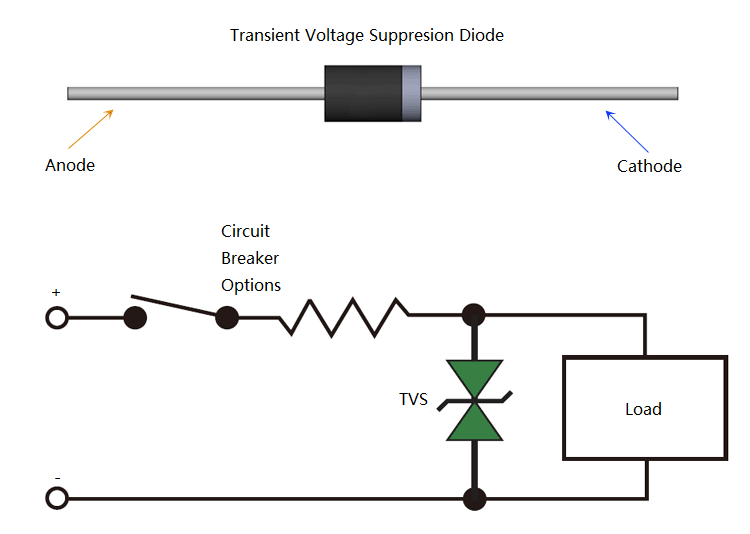
Transient Voltage Suppresison Diode
You May Also Like:
Features, Developemnt Trends and Disadvantages of Wireless Power Transfer
How to Reduce Electromagnetic Interference in Front-end Analog Devices
How to Judge Whether IC is Working Correctly in Electronic Circuit or Not
24 Classic Circuits Consisting of Bidirectional General Purpose Operational Amplifier LM358
Ordering & Quality
| Photo | Mfr. Part # | Company | Description | Package | Qty |
|
MR27V1602ETN | Company:OKI | Remark: | Package:TSOP |
MR27V1602ETN Datasheet |
In Stock:721 Inquiry |
Inquiry |
|
MPC8280VVQLDA | Company:NXP / Freescale | Remark:IC MPU MPC82XX 333MHZ 408TBGA | Package:480-LBGA |
MPC8280VVQLDA Datasheet |
In Stock:744 Inquiry |
Inquiry |
|
UPSD3212CV-24U6 | Company:STMicroelectronics | Remark:IC MCU 8BIT 80KB FLASH 80TQFP | Package:TQFP80 |
UPSD3212CV-24U6 Datasheet |
In Stock:1200 Inquiry |
Inquiry |
|
MCF52256AG80 | Company:NXP / Freescale | Remark:IC MCU 32BIT 256KB FLASH 144LQFP | Package:144-LQFP |
MCF52256AG80 Datasheet |
In Stock:2345 Inquiry |
Inquiry |
|
DSS16-01AS | Company:IXYS | Remark:DIODE SCHOTTKY 100V 16A TO263AB | Package:TO-263-3, D²Pak (2 Leads + Tab), TO- |
DSS16-01AS Datasheet |
In Stock:580 Inquiry |
Inquiry |
|
MC9S08GT16ACFBE | Company:NXP / Freescale | Remark:IC MCU 8BIT 16KB FLASH 44QFP | Package:QFP |
MC9S08GT16ACFBE Datasheet |
In Stock:746 Inquiry |
Inquiry |
|
MPY100CM | Company:TI | Remark:low cost precision device designed for general purpose application | Package:TO100 |
MPY100CM Datasheet |
In Stock:71 Inquiry |
Inquiry |
|
MCF51JM32VLK | Company:NXP | Remark:IC MCU 32BIT 32KB FLASH 80LQFP | Package:80-LQFP |
MCF51JM32VLK Datasheet |
In Stock:113 Inquiry |
Inquiry |
|
MC9S12C64CPBE | Company:NXP / Freescale | Remark:IC MCU 16BIT 64KB FLASH 52LQFP | Package:52-LQFP |
MC9S12C64CPBE Datasheet |
In Stock:2429 Inquiry |
Inquiry |
|
MPC8533EVTANG | Company:NXP / Freescale | Remark:IC MPU MPC85XX 800MHZ 783FCBGA | Package:783-BBGA, FCBGA |
MPC8533EVTANG Datasheet |
In Stock:79 Inquiry |
Inquiry |