25
How to Design DC-to-DC Converters
Principle 1
We should understand DC/DC power supply and DC/DC conversion circuit classification.
DC/DC power supply circuit is also known as DC/DC conversion circuit. Its main function is to carry out input/output voltage conversion.Generally we call the voltage transformation process of input power supply voltage within 72V DC/DC conversion. Common power supply is mainly divided into vehicle and communication series and general industrial and consumption series. The voltage used in the former is generally 48V, 36V, 24V, etc., while the voltage used in the latter is generally below 24V. Different application fields have different laws, such as 12V, 5V and 3.3v commonly used in PC, 5V and 15V commonly used in analog circuit power supply, and 3.3v commonly used in digital circuit. The current FPGA and DSP also use the voltage below 2V, such as 1.8v, 1.5v and 1.2v. Also known as secondary power supply in communication systems, it is a DC input voltage supplied by a primary power source or DC battery pack, which receives one or several DC voltages at the output end after DC/DC conversion.

DC/DC conversion circuits are mainly divided into the following three categories:
(1) The voltage regulator circuit of the zener diode.
(2) Linear (analog) voltage regulator circuit.
(3) Switch type voltage regulator circuit.
Principle 2
The simplest design scheme of zener diode.
The voltage regulator circuit is simple in structure, but with poor load capacity and small output power.
When choosing a zener diode, it can be estimated as follows:
(1) Uz=Vout;
(2) Izmax=(1.5-3)ILmax
(3) Vin=(2-3)Vout
This circuit structure is simple, and can inhibit the input voltage disturbance, but because it's limited by stabilivolt maximum working current, output voltage and can not be adjusted at the same time, so this circuit is suitable for occasions where the output voltage does not need to be adjusted, the load current is small, and the demand is not high.
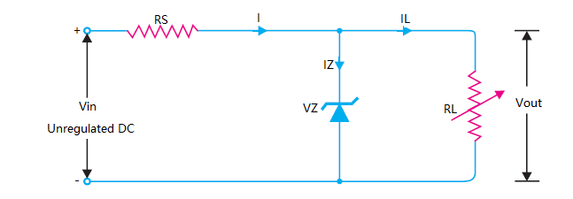
Zener Diode Voltage Regulator Circuit Diagram
Principle 3
In another form of the voltage regulator circuit, some chips have higher requirements on the supply voltage, such as the reference voltage of AD DA chip, etc. At this time, some common voltage reference chips such as TL431, MC1403,REF02, etc are used. TL431 is the most commonly used reference source chip, with good thermal stability of three-terminal adjustable split voltage source. Its output voltage can be arbitrarily set to any value between Vref(2.5v) and 36V with two resistances. Several other reference voltage source chip circuits are similar.

AD DA Conversion Modules
Principle 4
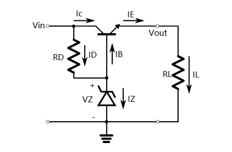
Knowledge of the circuit of series voltage regulator supply
Series voltage stabilizer is a kind of DC voltage stabilizer, which is actually a common DC power supply method before the emergence of the three-terminal voltage stabilizer. Before the emergence of the three-terminal voltage stabilizer, series voltage stabilizer usually has OP amplifier and voltage stabilizer diode to form an error detection circuit
Principle 5
A common design scheme for linear (analog) integrated voltage regulator circuits.
The linear voltage regulator circuit design is mainly based on three-terminal integrated voltage stabilizer. There are two main types of three-terminal voltage regulators:
The first type of output voltage is fixed, which is called fixed output three-terminal voltage stabilizer. The common product of three-terminal voltage stabilizer is series 78 (positive power supply) and series 79 (negative power supply). The output voltage is represented by the last two Numbers in the specific model, which are 5V, 6V, 8V, 9V, 12V, 15V, 18V, 24V and other grades. The output current is distinguished by a letter after 78(or 79).L means 0.1a,M means 0.5a, and no letters mean 1.5a. For example, in table 78L05, 5V is 0.1a.
The other output voltage is the adjustable linear voltage stabilizer, which is called the adjustable output three-terminal voltage regulator. This kind of chip represents the LM317(positive output) and LM337(negative output) series. The maximum input/output limit difference is 40V, the output voltage is 1.2v-35v (-1.2v --35V), the output current is 0.5-1.5a, the voltage between the output end and the adjustment end is 1.25v, and the static current of the adjustment end is 50uA.
These two basic principles are the same, both use series voltage regulator circuit. In the linear integrated voltage stabilizer, since the three-terminal voltage regulator has only three lead terminals, it has the advantages of less external components, easy to use, stable performance and low price, so it has been widely used.
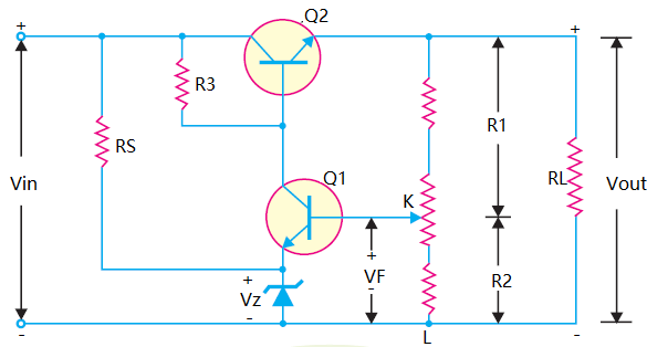
Linear Series Voltage Regulator
Principle 6
Design scheme of DC/DC switching voltage regulator circuit.
The DC/DC conversion circuits mentioned above all belong to the series feedback voltage regulator circuit. In this working mode, the regulating tube in the integrated voltage regulator works in the linear amplification state. Therefore, when the load current is large, the loss is relatively large, that is, the conversion efficiency is not high.Therefore, the power of the power supply circuit using the integrated voltage stabilizer is not very large, generally only 2-3w. This design scheme is only suitable for the low-power power supply circuit.
DC/DC converter circuit designed with switching power chip has high conversion efficiency and is suitable for larger power supply circuit. At present, it has been widely used, which is divided into non-isolated switch power supply and isolated switch power supply circuit.
DC/DC conversion switch voltage regulator circuit design scheme, DCDC conversion circuit designed by switching power chip is of high efficiency, suitable for larger power supply circuit. At present, it has been widely used, which is divided into non-isolated switch power supply and isolated switch power supply circuit. Of course, the basic topology of switching power supply includes step-down, step-up, up-down and flyback, positive, bridge change and so on.
Series Feedback Voltage Regulator
Principle 7
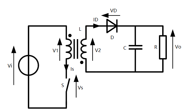
Design scheme of non - isolated DC/DC switching and switching IC chip.
DC/DC switch integrated circuit chips, the use of this kind of chip method is similar to the LM317 in the principle. We will take L4960 as an example here. They generally use 50 hz power transformer for AC - AC transformation, and then will be moved down ~ 220 v switching power supply integrated conversion chip such as input voltage range of 1.2 ~ 34 v, DC - DC by L4960 transformation, then under the range of output voltage can be adjusted to 5 v, increase to 40 v, maximum output current of 2.5 A (you can also pick up expansion of high power switch pipe flow), and with perfect protection function,Such as over - current protection, overheating protection and so on. Although the use method of L4960 is similar to that of LM317, the efficiency of switch power supply L4960 is different from that of linear power supply LM317. The maximum output power of L4960 can be 100W (Pmax=40V* 2.5A =100W), but it only consumes 7W at most, so the radiator is small and easy to make. Similar to L4960 is L296, which has the same basic parameters as L4960, but the maximum output current can be up to 4A, with more protection functions and different packaging forms. This kind of chip is more, for example, LM2576 series, TPS54350, LTC3770 and so on.Generally, the manufacturer will provide detailed instructions and typical circuits for reference when using these chips.
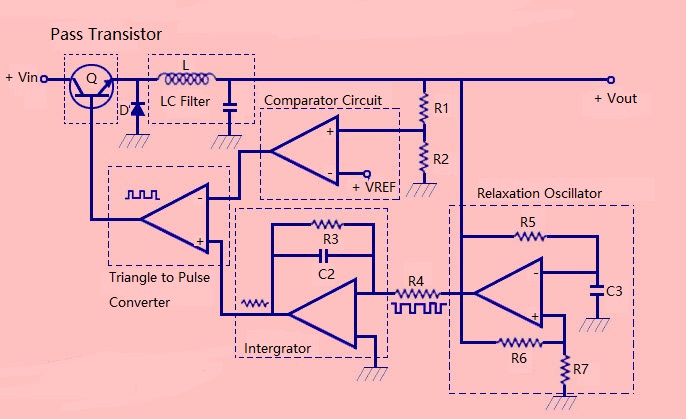
Switching Voltage Regulator
Principle 8
Design scheme of isolated DC/DC switching power supply module circuit.
The commonly used isolated DC/DC transformation is mainly divided into three categories:
(1) Flyback transformation
Schematic of a Flyback Converter
(2) Forward transformation
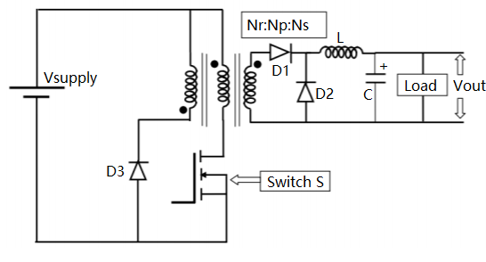
General Schematic of Forward Converter
(3) Bridge transformation
Wecommonly used single-end flyback DC/DC conversion circuit, this kind of isolated control chip model is also quite a few. The control chip is typically represented by the UC3842 series. This controller is a high performance fixed frequency current controller, which is mainly used to isolate AC/DC and DC/DC conversion circuits. Its main application principle is: the circuit is composed of main circuit, control circuit, startup circuit and feedback circuit. The main circuit adopts single-end flyback topology, which is composed of lifting voltage chopper circuit and isolation transformer after evolution. This circuit has the advantages of simple structure, high efficiency and wide input voltage range. The control circuit is the core of the whole switching power supply. This circuit adopts the peak-current two-loop control, that is, the peak current feedback control is added to the voltage closed-loop control system. The power of transformers and MOS tubes can be very large in this kind of scheme. Compared with the previous design schemes, the circuit structure is complex, the component parameters are difficult to determine, and the development cost is relatively high. Therefore, when this scheme is needed, the DC/DC isolation module which is relatively cheap in the market can be selected as the priority.
Principle 9
DC/DC switch integrated power module scheme
Many microprocessors and digital signal processors (DSP) require a kernel power supply and an input/output (I/O) power supply that must be sequenced at start up. Designers must consider the relative voltage and timing of the kernel and I/O voltage source during power-on and power-off operations to meet the manufacturer's performance specifications. Without proper power sequencing, latching or excessive current consumption can occur, which can result in I/O port or memory for microprocessors, programmable logic devices (PLD), field programmable gate arrays (FPGA), or I/O ports of support devices such as data converters being damaged.To ensure that I/O loads are not driven before the kernel voltage is properly offset, kernel power and I/O power tracing are required. There are now specialized power module companies custom-made some special switch power module, mainly for the DC/DC power module with small volume, high power density, high conversion efficiency, less heating, long average fault-free working time, good reliability, lower cost and higher performance besides the conventional electric performance index. These modules combine most or all of the components required to implement a plug-in solution and can replace up to 40 different components. This simplifies the integration and speeds up the design while reducing the power management portion of the board space.
A Simplified PAL Device
The most traditional and common non-isolated DC/DC power module is still a single in-line (SiP) package. These open framework solutions have indeed made progress in reducing design complexity. The simplest, however, is to use standard encapsulated components on printed circuit boards.
Principle 10
Notes for selecting DC/DC power conversion scheme.
This principle is a golden rule and also the important summary of this article. This paper mainly introduces three design methods of circuit modes, namely, DC/DC power conversion voltage regulator, linear (analog) voltage regulator, and DC/DC switching voltage regulator.Here are three notes needed our attention:
(1) The voltage regulator circuit can not be used for power supply, but only for chip without power requirement.
(2) The linear voltage regulator circuit with linear mode is simple in structure, but it can only be used in low-power voltage stabilized power supply due to low conversion efficiency.
(3) The switch type voltage regulator circuit with high conversion efficiency can be applied in high-power situations, but its limitation is relatively complex circuit structure(especially high-power circuit), which is not conducive to miniaturization.
Based on the above ten principles, we're able to choose a suitable design scheme according to actual needs in the design process.
You May Also Like:
Some Basic Knowledge of Solid Capacitors
What Are the Essential Differences Between PLC and Microcontrollers?
Selection of Residual Current Protector in Charging Pile
PCB Layout Tips and Tricks: The Components and Wires
Ordering & Quality
| Photo | Mfr. Part # | Company | Description | Package | Qty |
|
MAX6315US45D3+T | Company:Maxim Integrated | Remark:IC RESET CIRCUIT 4.50V SOT143-4 | Package:TO-253-4, TO-253AA |
MAX6315US45D3+T Datasheet |
In Stock:23310 Inquiry |
Inquiry |
|
BAT48 | Company:STMicroelectronics | Remark:DIODE SCHOTTKY 40V 350MA DO35 | Package:DO-204AH, DO-35, Axial |
BAT48 Datasheet |
In Stock:55560 Inquiry |
Inquiry |
|
MC9S08GT16CFBE | Company:NXP / Freescale | Remark:IC MCU 8BIT 16KB FLASH 44QFP | Package:44-QFP |
MC9S08GT16CFBE Datasheet |
In Stock:16320 Inquiry |
Inquiry |
|
MC9S12XDG128MAA | Company:NXP | Remark:IC MCU 16BIT 128KB FLASH 80QFP | Package:80-QFP |
MC9S12XDG128MAA Datasheet |
In Stock:126 Inquiry |
Inquiry |
|
FC4L110R050FER | Company:Ohmite | Remark:RES SMD 0.05 OHM 5W 4320 WIDE | Package:Wide 4320 (11050 Metric), 2043 |
FC4L110R050FER Datasheet |
In Stock:481 Inquiry |
Inquiry |
|
TMS320DM8127SCYED3 | Company:Texas Instruments | Remark:IC DGTL MEDIA PROCESSOR | Package:684-BFBGA, FCBGA |
TMS320DM8127SCYED3 Datasheet |
In Stock:433 Inquiry |
Inquiry |
|
MPC8544CVTALFA | Company:NXP / Freescale | Remark:IC MPU MPC85XX 667MHZ 783FCBGA | Package:BGA |
MPC8544CVTALFA Datasheet |
In Stock:69 Inquiry |
Inquiry |
|
RC0603FR-071KL | Company:Yageo | Remark:RES SMD 1K OHM 1% 1/10W 0603 | Package:SMD |
RC0603FR-071KL Datasheet |
In Stock:39061200 Inquiry |
Inquiry |
|
ATTINY13A-SUR | Company:Microchip | Remark:IC MCU 8BIT 1KB FLASH 8SOIC | Package:08LSOIJ |
ATTINY13A-SUR Datasheet |
In Stock:7060 Inquiry |
Inquiry |
|
MC9S08QA2CFQE | Company:NXP | Remark:IC MCU 8BIT 2KB FLASH 8QFN | Package:8-VDFN Exposed Pad |
MC9S08QA2CFQE Datasheet |
In Stock:25275 Inquiry |
Inquiry |