4
Introduction
For electronic products, printed circuit board design is a necessary part in electrical schematic diagram design procedure. The rationality of design is closely related to the production and the quality of the products. For many people who have just engaged in electronic design, they might have problems in the PCB design due to their lack of experience, although they have indeed learned many about how to do it. Considering i have been working in this field for many years, I would like to share some of my personal experience with all of you about how to design a PCB layout in the aspects of components and wiring.
How to make a Printed Circuit Board (PCB) at home
PCB Layout

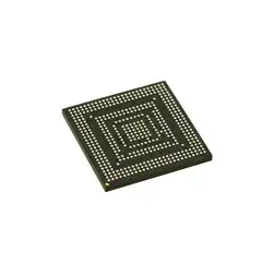
Figure 1 Printed Circuit Board Sample
To place components in the following basic order:

Figure 2 A series of Electronic Components
1. The fixed position components, such as power sockets, indicator lights, switches and connectors, which are placed in close coordination with the structure, will be locked with the LOCK function of the software so that they will not be moved by mistake later. In general, the interface between the power supply and the PCB is placed at the edge of the PCB and has a distance of 3 mm~5 mm to the edge of the PCB; indicates that the LED should be placed exactly as needed; switches and some fine-tuned components, such as adjustable inductors, variable resistors and so on should be placed near the edge of the PCB for easy adjustment and connection; components that need to be replaced frequently must be placed in fewer-components positions to be easily replaced.
2. Special components and large components are placed on the line, such as heating elements, transformer, IC(integrated circuit), etc. High power tubes, transformers, rectifiers and other heating devices produce more heat when they work at high frequency, so ventilation and heat dissipation should be fully considered in the layout, and these components should be placed in the place where the air can easily circulate on the PCB. High-power rectifier and adjustment tubes should be equipped with radiators and away from transformers. Thermal elements such as electrolytic capacitors should also be kept away from heating devices, otherwise the electrolyte will be dried up, resulting in the increase of its resistance and the deterioration of its performance, which will affect the stability of the circuit. Fault-prone components, such as adjusting tubes, electrolytic capacitors, relays and so on should consider the convenience of maintenance needs. For measuring test points, care should be taken to ensure that the test rods are easily accessible when arranging components.
3. Inductors, transformers and other devices have magnetic coupling, they should be placed orthogonal to reduce magnetic coupling. In addition, they all have a strong magnetic field where contains appropriate space or magnetic shielding around them to reduce the influence on other circuits.
Because the 50 Hz leakage magnetic field is produced inside the power supply, it will interfere with the low frequency amplifier when it is connected with some parts of the low frequency amplifier. Therefore, they must be separated or shielded. The amplifier at all levels can be arranged best in a straight line form according to the principle diagram. The advantage of this array is that the grounding current at all levels is closed, and the closed flow does not affect the operation of other circuits. Input and output stages should be as far away as possible to reduce parasitic coupling interference between them.
4. Appropriate high frequency decoupling capacitors should be arranged in the key parts of PCB, such as a 10 μF ~100 μF electrolytic capacitor at the input end of the PCB power supply, and a ceramic chip capacitance of about 0.01pF near the power pin of the integrated circuit. Some circuits are also equipped with appropriate high-frequency or low-frequency chokes to minimize the effect between high and low frequency circuits. This should be taken into account in schematic design and drawing, otherwise it will affect the performance of the circuit.
5. Place small devices. The distance from the edge of the board: all components are placed within 3mm of the edge of the board, or at least greater than the thickness of the board. If possible, as a result of being provided to the guideway slot for mass production of assembly lines and for peak soldering. At the same time, in order to prevent the defect of the edge part caused by the contour machining. If there are too many components on the printed circuit board and have to go beyond the scope of 3mm, we can add a 3mm auxiliary edge at the edge of the board and make a V-shaped groove on it., so that it’s easy to break.
6. Isolation between high and low voltage. On many printed circuit boards there are both high voltage and low voltage circuits. The components of the high voltage circuit are separated from the low voltage, and the isolation distance is related to the withstand voltage. Normally, the distance on the 2000kV board is 2 mm, which is proportional to that. For example, in order to withstand a voltage test of 3000 V, the distance between the high and low voltage wires should be above 3.5mm. In many cases to avoid creeping, there are slots in the printed circuit board between high and low voltage.
PCB Trace Routing
It is best to use a full line according to the direction of the signal, and 45 °curve or arc curve can be used to complete the circuit, which can reduce the external transmission of the high-frequency signal and the coupling between each other. High-frequency signal lines should be wired as short as possible. According to the working frequency of the circuit, the length of the signal wiring should be reasonably selected, which can reduce the distribution parameters and the loss of the signal. When making double panels, it is best to intersect, oblique or bend each other on two adjacent layers. Avoiding parallelism, which reduces mutual interference and parasitic coupling.
High-frequency signal lines and low-frequency signal lines should be separated as far as possible, and shielding measures should be taken if necessary to prevent interference between each other. For the weak signal input, it is easy to be interfered by the external signal, so the ground wire can be used to shield it or to shield the high frequency connector. Parallel lines should be avoided at the same level, otherwise the distribution parameters will be introduced, which will have an impact on the circuit. If it cannot be avoided, a grounded copper foil can be introduced between two parallel lines to form an isolated line.

Figure 3 Showing Some Routes of Conductor in PCB Design
The Width of Printed Conductors
In the process of PCB routing, the minimum width of the conductor is determined by the adhesion strength between the conductor and the insulating substrate and the current strength of the conductor. The conductor width should be suitable to meet the requirements of electrical performance and be convenient for production. Its minimum value should be determined by the current flow, but the minimum should not be less than 0.2 mm. In high density and high precision printed circuits, the conductor width and spacing can generally be 0.3 mm. The temperature rise of the wire is also considered in the case of high current. The results of single-sided plate experiment show that the temperature rise is very small when the thickness of copper foil is 50 μ m, the wire width is 1 ~ 1. 5 mm, and the temperature rise is not obvious when the current is 2A. Generally, the choice of 1~1.5mm width conductor may meet the design requirements without causing temperature rise.
The common ground wire of a printed wire should be as thick as possible, and if possible, larger than 2~3mm, which is particularly important in a circuit with a microprocessor. Thinner ground wire leads to the flowing current change, the ground potential variation and the unstable microprocessor timing signal which make the noise margin deteriorating. The 10-10 and 12-12 principles can be applied to the IC pins routing in DIP package, that is, when the two pins pass through two wires, the pad diameter can be set to 50mil(1.27mm), and the wire width and line distance are both 10mi(0.254mm); When the two pins pass only one wire, the pad diameter can be set to 64mil(1.626), and the wire width and distance are 12 mil( 0.305mm).

Figure 4 Showing the Relations of Thickness and Width of the Trace
Spacing between the Printed Conductors
The distance between adjacent wire must meet the requirements of electrical safety and should be as wide as possible for ease of operation and production. The minimum spacing must be at least suitable to withstand the voltage. This voltage generally includes operating voltage, additional fluctuation voltage, and peak voltage caused by other reasons. If the technical conditions permit the existence of a certain degree of metal residue between the conductors, the distance between them will decrease. Therefore, the designer should take this factor into account when considering voltage. When the wiring density is low, the distance between signal lines can be increased appropriately, and the distance between signal lines with high and low level disparity should be as short as possible while the spacing should be increased as much as possible.

Figure 5 Relations of Copper Foil Thickness, Conductor Width and Current
Shielding and Grounding of Printed Conductors
The common ground wire of printed wire should be arranged as far as possible on the edge of printed circuit board. Copper foils should be used as ground wires on the printed circuit board as much as possible, which is better than longer ground wires in the term of shielding effect, also improve transmission line characteristic and weaken the role of distributed capacitance.
Public ground wires for printed conductors are best formed in loops or reticulation to reduce grounding potential difference. The reason is that when there are many integrated circuits on the same board, especially those with more power consuming elements, grounding potential differences are formed due to graphical limitations, causing noise capacitance reduced, and grounding potential difference decreased when the circuit made.
In addition, the patterns of grounding and power supply should, as far as possible, be parallel to the flow direction of the data, which is the secret of increasing the ability to suppress noise. Multi-layer printed circuit boards can take several of themselves as shielding layers, like power and ground layers, general speaking,are designed in the inner part.
You May Also Like:
MOSFET Gate Drive Circuit Guidelines - Hints & Tips
The Sino-US Comparison in Information Technology
New Materials Selection Has Been An Trend
Common Guide for Selecting Electronic Components
Ordering & Quality
| Photo | Mfr. Part # | Company | Description | Package | Qty |
|
MCF51JM32VLK | Company:NXP | Remark:IC MCU 32BIT 32KB FLASH 80LQFP | Package:80-LQFP |
MCF51JM32VLK Datasheet |
In Stock:113 Inquiry |
Inquiry |
|
MK20DX256VLH7 | Company:NXP / Freescale | Remark:IC MCU 32BIT 256KB FLASH 64LQFP | Package:64-LQFP |
MK20DX256VLH7 Datasheet |
In Stock:5060 Inquiry |
Inquiry |
|
MMA2204KEGR2 | Company:Freescale Semiconductor - NXP | Remark:ACCELEROMETER 112.5G ANAL 16SOIC | Package:16-SOIC (0.295", 7.50mm Width) |
MMA2204KEGR2 Datasheet |
In Stock:1330 Inquiry |
Inquiry |
|
MC9S12C64CFAE | Company:NXP / Freescale | Remark:IC MCU 16BIT 64KB FLASH 48LQFP | Package:48-LQFP |
MC9S12C64CFAE Datasheet |
In Stock:615 Inquiry |
Inquiry |
|
MCIMX31LCVKN5D | Company:NXP / Freescale | Remark:IC MPU I.MX31 532MHZ 457MAPBGA | Package:457-LFBGA |
MCIMX31LCVKN5D Datasheet |
In Stock:147 Inquiry |
Inquiry |
|
K9F4G08UOA-P1BO | Company:SAMSUNG | Remark:4G-bit NAND Flash Memory with spare 128M-bit | Package: |
K9F4G08UOA-P1BO Datasheet |
In Stock:5960 Inquiry |
Inquiry |
|
MCF52210CEP66 | Company:NXP | Remark:IC MCU 32BIT 64KB FLASH 64QFN | Package:64-VFQFN Exposed Pad |
MCF52210CEP66 Datasheet |
In Stock:144 Inquiry |
Inquiry |
|
STTH12R06G-TR | Company:STMicroelectronics | Remark:DIODE GEN PURP 600V 12A D2PAK | Package:263AB |
STTH12R06G-TR Datasheet |
In Stock:11035 Inquiry |
Inquiry |
|
MPY100CM | Company:TI | Remark:low cost precision device designed for general purpose application | Package:TO100 |
MPY100CM Datasheet |
In Stock:71 Inquiry |
Inquiry |

|
Z8F042ASB020EG | Company:ZiLOG | Remark:IC MCU 8BIT 4KB FLASH 8SOIC | Package:8-SOIC (0.154", 3.90mm Width) |
Z8F042ASB020EG Datasheet |
In Stock:802 Inquiry |
Inquiry |