27
The author perfected this article on Jan 17, 2020
Abstract
As MOSFET is widely used today, it is necessary to comprehend how does MOSFET work and its basic knowledge. Metal oxide semiconductor field effect transistor (MOSFET) is a field-effect transistor (FET) that can be widely used in analog and digital circuits. According to the polarity of its "channel" (working carrier), MOSFET can be divided into two types: "N-type" and "P-type", which also called NMOSFET and PMOSFET or NMOS and PMOS. To know more about it, we should learn about its working principle, basic structures and other details.
Catalog
Abstract | |
I Introduction | |
II Structure of MOSFET | |
III Circuit Symbol of MOSFET | |
IV Working Principle of MOSFET | |
V MOSFET Applications & Advantages | 1. Digital Circuit |
2. Analog Circuit | |
VI Book Recommendation | |
I Introduction
Metal oxide semiconductor field effect transistor, also called (MOSFET) is a field-effect transistor (FET) that can be widely used in analog and digital circuits. From the point of the naming of MOSFET, it gives the wrong impression that the first letter M, which stands for "metal" in MOSFET and does not exist in most of today's components of its kind. The gate electrode of the early MOSFET used metal as its material, but with the development of semiconductor technology, polysilicon has replaced metal as the material of gate electrode of MOSFET. In processor, the Polysilicon gate is no longer the mainstream technology. Metal is reused in gate again after Intel using P1266 processor with 45nm line width.
MOSFET is conceptually "insulated gate field effect transistor"(IGFET). The gate insulator of IGFET may be the oxide layer used by other substances rather than by MOSFET. Some people prefer IGFETs when it comes to field-effect transistors with polysilicon gates, but most of these IGFET refer to MOSFETs.
MOSFET Basics
Today, silicon is the preferred material for semiconductor components, but some semiconductor companies have developed processes using other semiconductor materials, the most famous one being the silicon-germanium process( SiGe process ) developed by IBM using a mixture of silicon and germanium. Unfortunately, many semiconductor materials with good electrical properties, such as gallium arsenide (GaAs), cannot be used to make MOSFET components because they cannot produce enough oxide layer on the surface.
When a sufficiently large potential difference is applied between the gate and the source of the MOSFET, the electric field forms an inductive charge on the surface of the semiconductor beneath the oxide layer, and the so-called "inversion channel" is formed. The polarity of the channel is the same as that of the source. Assuming that the drain and source are N-type, then the channel will also be N-type. After the channel is formed, MOSFETs can allow the current to pass through. According to the voltage applied on the gate, the current that can flow through the channel of MOSFET is also controlled by the MOSFET.
MOSFET is a kind of unipolar voltage controlled semiconductor device. The gate DC input impedance of it is extremely high. It has the characteristics of low driving power, high switching speed, no secondary breakdown, wide safe area, and the switching frequency is higher than 500KH, therefore, it is especially suitable for high frequency devices. However MOSFET can only be used in medium and small power devices because of its small current capacity and low voltage resistance.
II Structure of MOSFET

MOSFET Structure
1. Source: Source of majority carriers (P-hole, N-electron)
2. Drain: Endpoints that accept these majority carriers
3. Gate: Composite of poly-silicon. Accept positive voltage at NMOSFET and negative voltage at PMOSFET
4. Bulk/Body: It can be divided into P type semiconductor doping and N type semiconductor doping in the base.

N-channel MOSFET Structure
Take the picture above as an example. The picture is a basic structure diagram of typical plane N-Channel enhanced NMOSFET. It uses a P-type silicon semiconductor material as a substrate, diffuses two N-type regions on its surface, then covers it with a layer of SiO2 insulator. Finally, two holes are made by corrosion over the N-region. Three electrodes were fabricated by metallization on the insulating layer and in two holes, which are Gate(G), Source(S), Drain(D). From the picture, we can find that gate is insulated from drain and source. There are two PN junctions between D and S. In general, the substrate and the source are connected internally, which is equivalent to a PN junction between D and S. In order to improve the characteristics of some parameters, such as increasing the working current, increasing the working voltage, reducing the on-resistance, improving the switching characteristics and so on, there are different structures and processes to form the so-called VMOS / DMOS / TMOS structure. Although there are different structures, their working principle is almost the same.
III Circuit Symbol of MOSFET
There are many variations in the symbols of circuits commonly used in MOSFET. The most common design is to represent the channel with a straight line, two lines perpendicular to the channel to represent the source and drain, and a parallel and shorter line on the left to represent the gate. Sometimes a line representing a channel is replaced by a broken line to distinguish between enhancement mode MOSFET or depletion mode MOSFET. In addition, it is divided into two types: NMOSFET and PMOSFET. The circuit symbols are shown in the figure below. Because the MOSFET on the IC chip is a four-terminal component, there is also a base (bulk or body), in addition to the gate, source and drain. In the symbol of the MOSFET circuit, the arrow extending from the channel to the right can represent the MOSFETs of N type or P type. The arrow direction always points from the P end to the N end, so the arrow points from the channel to the base extreme of the P-type MOSFET, or PMOS. On the contrary, if the arrow points from the bulk to the channel , then the bulk is P-type, and the channel is N-type, which is referred to as NMOS. In general distributed MOSFET components (discrete device), the bulk is usually connected to the source, so distributed MOSFET is usually a three-terminal component. The MOSFET in an integrated circuit usually uses a common bulk so that there will be no mark of the polarity of the base, but adds an extra circle to the gate of the PMOS to show the difference. In this way, MOSFET has four clock type: P channel enhancement mode, P channel depletion mode, N channel enhancement mode and N channel depletion mode. Their circuit symbols and application characteristic curves are shown in the following figure.

Circuit Symbol
IV Working Principle of MOSFET
The metal-oxidation-semiconductor structure MOSFET is structurally centered on the capacitance of a metal-oxide-semiconductor (as mentioned above, most of today's MOSFET uses polysilicon instead of metal as its gate material). Most of the oxide materials are silicon dioxide. Below it is silicon as a base, and on top it is polysilicon, which acts as a gate. This type of structure is exactly the same as a capacitor, and the oxide layer acts as the dielectric material of the capacitor. The capacitance is determined by the thickness of the oxide and the dielectric constant of silicon dioxide. The gate polysilicon and the base silicon are the two endpoints of the MOS capacitor.

Working Principle
When a voltage is applied to both ends of the MOS capacitor, the charge distribution of the semiconductor also changes. Consider the MOS capacitance formed by a P-type semiconductor (hole concentration is NA). When a positive voltage VGB is applied to the gate and base extremes, the hole concentration will decrease and the electron concentration will increase. When the VGB is strong enough, the electron concentration near the gate end will exceed the hole. In P-type semiconductors, the region where the electron concentration (negative charge) exceeds the hole (positive charge) concentration is the so-called inversion layer.
The characteristics of MOS capacitors determine the operating characteristics of MOSFET, but a complete MOSFET structure also requires a source that provides majority carriers and drains that receive these majority carriers.
In the picture above, to make the enhancement N-channel MOSFET work, it should add positive voltage VGS between the G and S and positive voltages VDS between D and S, which will generate positive current ID.
If the VGS (VGS=0) is not attached first, a positive voltage VDS is added between D and S, and the PN junction between D and the substrate is in the reverse, so the leakage source cannot be conductive. If a voltage VGS is added between the gate and the source, the gate and substrate can be regarded as the two polar plates of the capacitor, while the oxide insulating layer is used as the medium of the capacitor. When VGS is added, positive charges are induced at the insulator and gate interface, and negative charges are induced at the interface between the insulating layer and the P-type substrate. The induced negative charge in this layer is opposite to the polarity of most carriers (holes) in P-type substrates, so it is called the "inversion layer", which may connect the leakage to the two N-type regions of the source to form a conductive channel.When the VGS voltage is too low, the induced negative charge is less, and it will be neutralized by holes in the P-type substrate, so in this situation, there is still no current ID between the drain sources. When VGS is increased to a certain value, its induced negative charge communicates two separate N regions to form N channel. This critical voltage is called cut-in voltage (or threshold voltage), which is expressed by symbol VT ( VT is the VGS when ID=10uA ).

Operating Mode
When VGS continues to increase, the negative charge increases, the conductive channel expands, the resistance decreases while the ID increases. And there is a good linear relationship, which is called conversion characteristic. Therefore, in a certain range, it can be considered that changing the VGS to control the resistance between the drain-source to achieve the function of controlling the ID. Because this kind of structure is called enhancement MOSFET when VGS = 0. The other kind of MOSFETs with a certain ID(IDSS) at VGS = 0 is called depletion MOSFET.
The main difference between the depletion type and the enhanced type is that there are a large number of positive ions in the fabrication of the SiO2 insulating layer, which induces more negative charges on the interface of the P-type substrate. That is, a thin layer of N-type silicon is formed in the P-type silicon in the middle of two N-type regions to form a conductive channel. So, when VGS = 0, there is a certain ID when there is a VDS. When the VGS has a voltage (either a positive voltage or a negative voltage), it will change the number of negative charges induced to change the size of the ID. VP is -VGS when ID = 0, called pinch-off voltage.
V MOSFET Applications & Advantages
1. Digital Circuit
The advancement of digital technology, such as the improvement of microprocessor computing efficiency, brings more power to the further research and development of the new generation MOSFET, which makes the operation speed of MOSFET itself faster and faster, and almost become one of the fastest of all kinds of semiconductor active components.
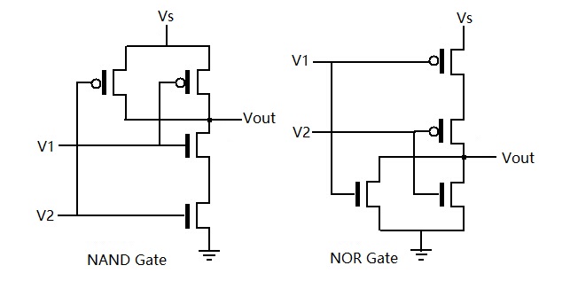
The major success of MOSFET in digital signal processing comes from the invention of CMOS logic circuit. The biggest advantage of this structure is that there is no static power loss in theory, and only when the switch of logic gate there is current passing through. The most basic member of the CMOS logic gate is the CMOS inverter. The basic operations of all CMOS logic gates are like inverters. There must be only one transistor, either NMOS or PMOS, in the state of conduction at the same time in the instant of logic conversion, and the other must be in a cut-off state. This results no direct path from the power source to the ground, which saves the current or power consumption, and reduces the heat of integrated circuit.
Another advantage of MOSFET applications in digital circuits is that for DC signals, the gate extreme impedance of MOSFET is infinite (equivalent to open circuit). That is, in theory, there will be no current flowing from the gate extreme of the MOSFET to the grounding point in the circuit, but in the form of a voltage-controlled gate. This makes MOSFET more power efficient and easier to drive than their main rival, BJT. In CMOS logic circuits, apart from driving off-chip load-driven drivers, each level of logic gate only has to face the same gate of MOSFET. In this way, there is no need to consider the driving force of the logic gate itself. By comparison, BJT logic circuits (such as the most common TTL) do not have these advantages. The infinite gate input resistance of MOSFET also has other advantages for circuit design engineers, such as less need to consider the loading effect of logic gate output.
CMOS Logic Circuits
2. Analog Circuit
MOSFETs are not the first choice for analog circuit design engineers for some time because MOSFETs are less suitable for analog circuits than BJT in terms of their performance parameters such as transistor transconductance or current driving forces. However, with the development of MOSFET technology, today's CMOS technology can meet the requirements of many analog circuits. In addition, MOSFET doesn't have some fatal weaknesses of BJT such as thermal runaway due to its structure. The voltage-controlled resistance characteristics of MOSFET in the linear region can also be used to replace the conventional polysilicon resistor in integrated circuits, or the MOS capacitor itself can be used to replace the commonly used PIP capacitors. These are benefits that BJT can not easily offer. In other words, MOSFET can also be used as a passive device in analog circuits, in addition to the role of the original transistor. The advantages of using MOSFET to realize analog circuit can not only meet the requirements of specifications, but also effectively reduce the chip area and production cost.
With the development of semiconductor manufacturing technology, the demand for integrating more functions into a single chip has increased dramatically. In this situation, we can found another advantage of using MOSFET to design analog circuits. In order to reduce the number of integrated circuits used on printed circuit boards (PCB) and to reduce the cost of packaging and the size of the system, many previously independent analog chips and digital chips were integrated into the same chip. MOSFET originally had a great competitive advantage in digital integrated circuits, and MOSFET was widely used in analog integrated circuits. After that, the difficulty of integrating these two kinds of circuits with different functions has also decreased significantly. In addition, some mixed signal circuits, such as Analog-to-Digital converters (ADC), have also been able to design more efficient products using MOSFET technology.
There is also a process technology that integrates the advantages of MOSFET and BJT: BiCMOS (Bipolar-CMOS), which is also becoming more and more popular. BJT components are still superior to conventional CMOS in their ability to drive large current, and have some advantages in reliability, such as being not easily damaged by "electrostatic discharge" (ESD). BJT is still superior to the average CMOS in its ability to drive large currents, and it also has some advantages in terms of reliability. For example, it is not easy to be damaged by "electrostatic discharge" (ESD). Therefore, many integrated circuit products that require complex noise number processing and strong current-drive capability will be made using BiCMOS technology.
VI Book Recommendation
1. MOSFET Theory and Design
Developed for a one-semester course at the junior, senior, or graduate level, MOSFET Theory and Design presents a clear, in-depth treatment of physical analysis and design principles for the MOSFET. By focusing solely on the MOSFET, this slim volume recognizes the dominance of this device in today's microelectronics technology while also providing students with an efficient text free of extra subject matter.
--R. M. Warner
2. Advanced Power MOSFET Concepts
During the last decade many new concepts have been proposed for improving the performance of power MOSFETs. The results of this research are dispersed in the technical literature among journal articles and abstracts of conferences. Consequently, the information is not readily available to researchers and practicing engineers in the power device community. There is no cohesive treatment of the ideas to provide an assessment of the relative merits of the ideas.
--B. Jayant Baliga
You May Also Like:
MOSFET Gate Drive Circuit Guidelines - Hints & Tips
Ordering & Quality
| Photo | Mfr. Part # | Company | Description | Package | Qty |

|
MC908QB4CDWE | Company:NXP | Remark:IC MCU 8BIT 4KB FLASH 16SOIC | Package:16-SOIC (0.295", 7.50mm Width) |
MC908QB4CDWE Datasheet |
In Stock:3816 Inquiry |
Inquiry |
|
MCIMX353DJQ5C | Company:NXP / Freescale | Remark:IC MPU I.MX35 532MHZ 400MAPBGA | Package:400-LFBGA |
MCIMX353DJQ5C Datasheet |
In Stock:24833 Inquiry |
Inquiry |
|
MC9S08GT16CFBE | Company:NXP / Freescale | Remark:IC MCU 8BIT 16KB FLASH 44QFP | Package:44-QFP |
MC9S08GT16CFBE Datasheet |
In Stock:16320 Inquiry |
Inquiry |

|
MC9S08QD4CSC | Company:NXP | Remark:IC MCU 8BIT 4KB FLASH 8SOIC | Package:SOIC8 |
MC9S08QD4CSC Datasheet |
In Stock:41393 Inquiry |
Inquiry |
|
MC68CK16Z1CAG16 | Company:NXP | Remark:IC MCU 16BIT 144LQFP | Package:144-LQFP |
MC68CK16Z1CAG16 Datasheet |
In Stock:18655 Inquiry |
Inquiry |
|
MCIMX6U5DVM10AC | Company:NXP / Freescale | Remark:IC MPU I.MX6DL 1.0GHZ 624MAPBGA | Package:624-LFBGA |
MCIMX6U5DVM10AC Datasheet |
In Stock:3160 Inquiry |
Inquiry |
|
MC9S12DG256MPVE | Company:NXP / Freescale | Remark:IC MCU 16BIT 256KB FLASH 112LQFP | Package:112-LQFP |
MC9S12DG256MPVE Datasheet |
In Stock:634 Inquiry |
Inquiry |
|
MAX6315US45D3+T | Company:Maxim Integrated | Remark:IC RESET CIRCUIT 4.50V SOT143-4 | Package:TO-253-4, TO-253AA |
MAX6315US45D3+T Datasheet |
In Stock:23310 Inquiry |
Inquiry |

|
MAX6804US29D2+T | Company:Maxim Integrated | Remark:Processor Supervisor 2.93V 2.85V to 5V 4-Pin(3+Tab) SOT-143 T/R | Package:TO-253-4, TO-253AA |
MAX6804US29D2+T Datasheet |
In Stock:8225 Inquiry |
Inquiry |
|
MRF18060B | Company:MOT | Remark: | Package:SMD |
MRF18060B Datasheet |
In Stock:71 Inquiry |
Inquiry |