| Manufacturer Part#: | MRF18060B |
| Product Category: | IC chips |
| Manufacturer: | MOT |
| Description: | |
| Package: | SMD |
| Quantity: | 71 PCS |
| Lead Free Status / RoHS Status: | Lead free / RoHS Compliant |
| one to seven days | |
| Click buy button to purchase: | Buy |
DESCRIPTION
RF Power Field Effect Transistors
N-Channel Enhancement-Mode Lateral MOSFETs
Designed for PCN and PCS base station applications with frequencies from 1.8 to 2.0 GHz. Suitable for FM, TDMA, CDMA and multicarrier amplifier applications. To be used in Class AB for PCN-PCS/cellular radio and WLL applications. Specified for GSM1930 - 1990 MHz.
• GSM Performance, Full Frequency Band (1930 - 1990 MHz),Power Gain ó 13 dB (Typ) @ 60 Watts CW, Efficiency ó 45% (Typ) @ 60 Watts CW
• Internally Matched, Controlled Q, for Ease of Use
• High Gain, High Efficiency and High Linearity
• Integrated ESD Protection
• Designed for Maximum Gain and Insertion Phase Flatness
• Capable of Handling 10:1 VSWR, @ 26 Vdc, 60 Watts CW Output Power
• Excellent Thermal Stability
• Available with Low Gold Plating Thickness on Leads. L Suffix Indicates 40µ″ Nominal.
• In Tape and Reel. R3 Suffix = 250 Units per 56 mm, 13 Inch Reel.
APPLICATION
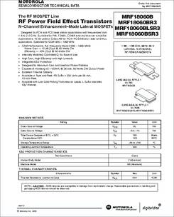
MRF18060B RF Power Field Effect Transistors MRF18060BR3 N-Channel Enhancement-Mode Lateral MOSFETs MRF18060BLSR3 Designed for PCN and PCS base station applications with frequencies from to 2.0 GHz. Suitable for FM, TDMA, CDMA and multicarrier amplifier applications. To be used in Class AB for PCN-PCS/cellular radio and WLL applications. Specified for - 1990 MHz. GSM Performance, Full Frequency Band - 1990 MHz) Power Gain 13 dB (Typ) @ 60 Watts CW Efficiency 45% (Typ) @ 60 Watts CW Internally Matched, Controlled Q, for Ease of Use High Gain, High Efficiency and High Linearity Integrated ESD Protection Designed for Maximum Gain and Insertion Phase Flatness Capable of Handling 10:1 VSWR, @ 26 Vdc, 60 Watts CW Output Power Excellent Thermal Stability Available in Tape and Reel. R3 Suffix = 250 Units per 56 mm, 13 Inch Reel. Available with Low Gold Plating Thickness on Leads. L Suffix Indicates 40μ Nominal. - 1.99 GHz, 26 V LATERAL N-CHANNEL RF POWER MOSFETs Rating Drain-Source Voltage Gate-Source Voltage Total Device Dissipation = 25°C Derate above 25°C Storage Temperature Range Operating Junction Temperature Symbol VDSS VGS PD Tstg TJ Value +150 200 Unit Vdc Watts W/°C °C Test Conditions Human Body Model Machine Model Class 2 (Minimum) M3 (Minimum) Characteristic Thermal Resistance, Junction to Case Symbol RJC Max 0.97 Unit °C/W.
NOTE - CAUTION - MOS devices are susceptible to damage from electrostatic charge. Reasonable precautions in handling and packaging MOS devices should be observed.
FEATURES
Characteristic OFF CHARACTERISTICS Drain-Source Breakdown Voltage (VGS = 0 Vdc, = 10 μAdc) Zero Gate Voltage Drain Current (VDS = 26 Vdc, VGS = 0 Vdc) Gate-Source Leakage Current (VGS = 5 Vdc, VDS = 0 Vdc) ON CHARACTERISTICS Gate Threshold Voltage (VDS = 10 Vdc, = 300 μAdc) Gate Quiescent Voltage (VDS = 26 Vdc, = 500 mAdc) Drain-Source On-Voltage (VGS = 10 Vdc, = 2 Adc) Forward Transconductance (VDS = 10 Vdc, = 2 Adc) DYNAMIC CHARACTERISTICS Input Capacitance (Including Input Matching Capacitor in Package) (1) (VDS = 26 Vdc ± 30 mV(rms)ac @ 1 MHz, VGS = 0 Vdc) Output Capacitance (1) (VDS = 26 Vdc ± 30 mV(rms)ac @ 1 MHz, VGS = 0 Vdc) Reverse Transfer Capacitance (VDS = 26 Vdc ± 30 mV(rms)ac @ 1 MHz, VGS = 0 Vdc) FUNCTIONAL TESTS (In Motorola Test Fixture, 50 ohm system) Common-Source Amplifier Power Gain W (2) (VDD = 26 Vdc, IDQ = 500 mA, f MHz) Drain Efficiency W (2) (VDD = 26 Vdc, IDQ = 500 mA, f MHz) Input Return Loss (2) (VDD = 26 Vdc, Pout 60 W CW, IDQ = 500 mA, f MHz) Output Mismatch Stress (VDD = 26 Vdc, Pout 60 W CW, IDQ 500 mA VSWR = 10:1, All Phase Angles at Frequency of Tests) Gps 11.5 40 IRL % dB Ciss Coss Crss 2.7 pF VGS(th) VGS(Q) VDS(on) gfs Vdc S V(BR)DSS IDSS IGSS 6 1 Vdc μAdc Symbol Min Typ Max Unit
No Degradation In Output Power Before and After Test
(1) Part is internally matched both on input and output. (2) To meet application requirements, Motorola test fixtures have been designed to cover the full GSM1900 band, ensuring batch-to-batch consistency.
10 pF, 100B Chip Capacitors 10 mF, 35 V Electrolytic Tantalum Capacitor 1.2 pF, 100B Chip Capacitors 1.0 pF, 100B Chip Capacitor 2.2 pF, 100B Chip Capacitor 0.3 pF, 100B Chip Capacitors 10 k Chip Resistors 1.0 k Chip Resistor (0805)
x 0.09 Microstrip x 0.09 Microstrip x 0.94 Microstrip x 0.98 Microstrip x 0.09 Microstrip x 0.09 Microstrip x 0.09 Microstrip Teflon Glass
SPECIFICATION
| Manufacturer | MOT |
| Product Category | IC Chips |
RELEVANT POPULAR RESEARCHES
| MRF18085A | MRF18085A |
| MRF18060B Datasheet | MRF18060B Price |
MRF18060B Inventory | MRF18060B Part |
PICTURE

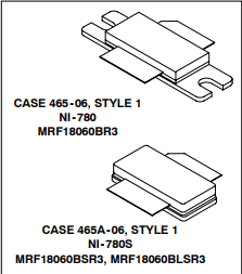

MRF18060B image
 IC RS485/RS422 DATA INTRFC 24DIP
 low cost precision device designed for general purpose application
 CAP CER 0.022UF 50V X7R RADIAL