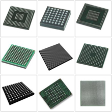
| Manufacturer Part#: | W631GG6KB-15 |
| Product Category: | Memory |
| Manufacturer: | Winbond Electronics |
| Description: | IC DRAM 1G PARALLEL 96WBGA |
| Package: | FBGA |
| Quantity: | 3070 PCS |
| Lead Free Status / RoHS Status: | Lead free / RoHS Compliant |
| one to seven days | |
| Click buy button to purchase: | Buy |
CAD Models
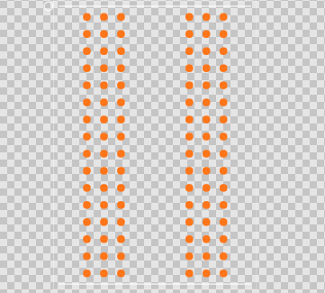
W631GG6KB-15 Footprint
Lifecycle Status Indicator
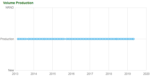
W631GG6KB-15 Lifecycle Status Indicator
Product Attributes
Manufacturer | WINBOND |
Product Category | Memory |
Access Time | 255 ps |
Access Mode | MULTI BANK PAGE BURST |
Address Bus Width | 16 b |
Data Bus Width | 16 b |
Density | 1 Gb |
DRAM Type | DDR3 SDRAM |
Frequency | 667 MHz |
Interface | Parallel |
Interleaved Burst Length | 8 |
I/O Type | COMMON |
JESD-30 Code | R-PBGA-B96 |
Lead Finish(Plating) | SnAgCu |
Lead Shape | Ball |
Mount Type | Surface Mount |
Maximum Clock Rate | 1333 MHz |
Maximum Random Access Time | 20 ns |
Maximum Reflow Temperature | 260 °C |
Reflow Solder Time (Sec) | 20 to 40 |
Maximum Operating Temperature | 85 °C |
Minimum Operating Temperature | 0 °C |
Maximum Operating Current | 130 mA |
Maximum Standby Current | 0.014 Amp |
Maximum Supply Current | 0.38 Amp |
Typical Supply Voltage | 1.5 V |
Maximum Supply Voltage | 1.575 V |
Minimum Supply Voltage | 1.425 V |
Memory Type | RAM, DDR3 SDRAM |
Memory Density | 1.073741824E9 bit |
Memory Width | 16 |
Nominal Supply Current | 240 mA |
Number of Functions | 1 |
Number of Ports | 1 |
Number of I/O Lines | 16 bit |
Number of Internal Banks | 8 |
Number of Words per Bank | 8M |
Number of Words | 6.7108864E7 words |
Number of Words Code | 64 M |
Operating Mode | SYNCHRONOUS |
Organization | 64Mx16 |
Operating Temperature Classification | Commercial |
Output Characteristics | 3-STATE |
Packaging | Tray |
Package / Case | 96-TFBGA |
Mfr Package Description | WBGA-96 |
Package Body Material | PLASTIC/EPOXY |
Package Code | TFBGA |
Package Equivalence Code | BGA96,9X16,32 |
Package Shape | RECTANGULAR |
Package Style | GRID ARRAY, THIN PROFILE, FINE PITCH |
Package Dimensions | 9 x 13 x 0.8 mm |
Package Length | 13 mm |
Package Width | 9 mm |
Package Height | 0.8(Max) mm |
Pin Count | 96 |
PCB | 96 |
Pin Pitch | 0.8 mm |
Power Supplies | 1.5 V |
Refresh Cycles | 8192 |
Sub Category | DRAMs |
Supplier Device Package | 96-WBGA (9x13) |
Sequential Burst Length | 8 |
Seated Plane Height | 1.2(Max) mm |
Technology | CMOS |
Temperature Grade | OTHER |
Terminal Form | BALL |
Additional Feature | AUTO/SELF REFRESH |
GENERAL DESCRIPTION
The W631GG6KB is a 1G bits DDR3 SDRAM, organized as 8,388,608 words x 8 banks x 16 bits. This device achieves high speed transfer rates up to 1866 Mb/sec/pin (DDR3-1866) for various applications. The W631GG6KB is sorted into the following speed grades: -11, 11I, -12, 12I, 12J, -15, 15I and 15J. The -11 and 11I speed grades are compliant to the DDR3-1866 (13-13-13) specification (The 11I industrial grade which is guaranteed to support -40°C ≤ TCASE ≤ 95°C). The -12, 12I and 12J speed grades are compliant to the DDR3-1600 (11-11-11) specification (The 12I industrial grade which is guaranteed to support -40°C ≤ TCASE ≤ 95°C, the 12J industrial plus grade which is guaranteed to support -40°C ≤ TCASE ≤ 105°C). The -15, 15I and 15J speed grades are compliant to the DDR3-1333 (9-9-9) specification (The 15I industrial grade which is guaranteed to support -40°C ≤ TCASE ≤ 95°C, the 15J industrial plus grade which is guaranteed to support -40°C ≤ TCASE ≤ 105°C). The W631GG6KB is designed to comply with the following key DDR3 SDRAM features such as posted CAS#, programmable CAS# Write Latency (CWL), ZQ calibration, on die termination and asynchronous reset. All of the control and address inputs are synchronized with a pair of externally supplied differential clocks. Inputs are latched at the cross point of differential clocks (CK rising and CK# falling). All I/Os are synchronized with a differential DQS-DQS# pair in a source synchronous fashion.
Features
● Power Supply: VDD, VDDQ = 1.5V ± 0.075V
● Double Data Rate architecture: two data transfers per clock cycle
● Eight internal banks for concurrent operation
● 8 bit prefetch architecture
● CAS Latency: 6, 7, 8, 9, 10, 11 and 13
● Burst length 8 (BL8) and burst chop 4 (BC4) modes: fixed via mode register (MRS) or selectable OnThe-Fly (OTF)
● Programmable read burst ordering: interleaved or nibble sequential
● Bi-directional, differential data strobes (DQS and DQS#) are transmitted / received with data
● Edge-aligned with read data and center-aligned with write data
● DLL aligns DQ and DQS transitions with clock
● Differential clock inputs (CK and CK#)
● Commands entered on each positive CK edge, data and data mask are referenced to both edges of a differential data strobe pair (double data rate)
● Posted CAS with programmable additive latency (AL = 0, CL - 1 and CL - 2) for improved command, address and data bus efficiency
● Read Latency = Additive Latency plus CAS Latency (RL = AL + CL)
● Auto-precharge operation for read and write bursts
● Refresh, Self-Refresh, Auto Self-refresh (ASR) and Partial array self refresh (PASR)
● Precharged Power Down and Active Power Down
● Data masks (DM) for write data
● Programmable CAS Write Latency (CWL) per operating frequency
● Write Latency WL = AL + CWL
● Multi purpose register (MPR) for readout a predefined system timing calibration bit sequence
● System level timing calibration support via write leveling and MPR read pattern
● ZQ Calibration for output driver and ODT using external reference resistor to ground
● Asynchronous RESET# pin for Power-up initialization sequence and reset function
● Programmable on-die termination (ODT) for data, data mask and differential strobe pairs
● Dynamic ODT mode for improved signal integrity and preselectable termination impedances during writes
● 2K Byte page size
● Interface: SSTL_15
● Packaged in WBGA 96 Ball (9x13 mm2 ), using lead free materials with RoHS compliant
Advantages and Disadvantages
There is no relevant information available for this part yet.
Applications
There is no relevant information available for this part yet.
ECCN / UNSPSC
Description | Value |
ECCN | EAR99 |
HTSN | PARTS... |
SCHEDULE B | PARTS... |
Documents & Media
Datasheet |
Product Manufacturer
Winbond was established in September 1987 and listed on Taiwan Stock Exchange in 1995 with headquarters in Central Taiwan Science Park, Taichung, Taiwan.
Winbond Electronics Corporation is a memory IC company engaged in design, manufacturing and sales service to provide its global customers top quality memory solutions. Winbond’s product lines include Code Storage Flash Memory, Serial and Parallel NAND, Specialty DRAM and Mobile DRAM.
Winbond products are widely used by companies in the IoT vertical markets such as computing, connected multimedia devices, automobile, networking systems and industrial. Winbond offers automotive and Industrial –Plus grade Flash and DRAM products with longevity support. Winbond has approximately 2,200 employees worldwide, that includes a 12-inch FAB at its headquarters in Taichung, Taiwan.
Product Range
Mobile DRAM | Pseudo SRAM | Low Power SDR SDRAM |
Specialty DRAM | SDRAM | DDR SDRAM |
Code Storage Flash Memory | Serial NOR Flash | 1.2V Serial NOR Flash |
Distributors
Distributors | Stock | Manufacturers | Descriptions |
Kynix | 3070 | WINBOND | IC DRAM 1G PARALLEL 96WBGA |
DigiKey | 0 | Winbond Electronics | SDRAM - DDR3 Memory IC 1Gb (64M x 16) Parallel 667MHz 20ns 96-WBGA (9x13) |
Arrow | 50 | Winbond Electronics | DRAM Chip DDR3 SDRAM 1Gbit 64Mx16 1.5V 96-Pin WBGA |
Avnet | 0 | Winbond | DRAM Chip DDR3 SDRAM 1G-Bit 64Mx16 1.5V 96-Pin W-BGA |
Alternative Models
There is no relevant information available for this part yet.
Popularity by Region
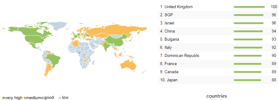
W631GG6KB-15 Popularity by Region
Market Price Analysis
There is no relevant information available for this part yet.
 SRAM 128K x 36 Synchronous Bank-Switchable Dual-Port SRAM
 4G-bit NAND Flash Memory with spare 128M-bit
 consumer memory