| Manufacturer Part#: | MC9S08LL8CGT |
| Product Category: | Embedded - Microcontrollers |
| Manufacturer: | NXP |
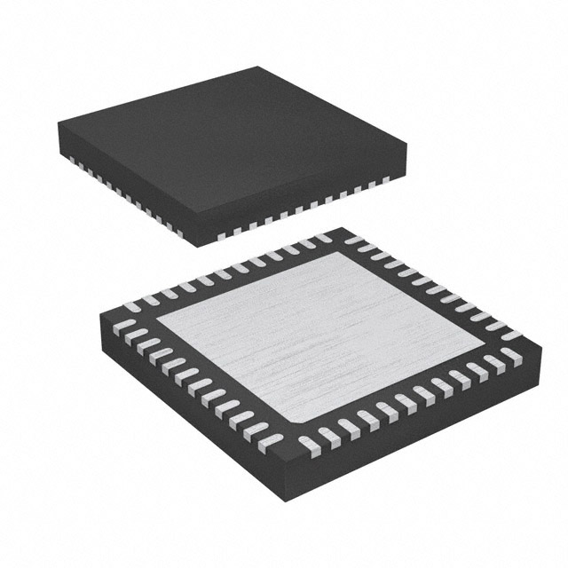
| Description: | IC MCU 8BIT 10KB FLASH 48QFN |
| Package: | 48-VFQFN Exposed Pad |
| Quantity: | 3739 PCS |
| Lead Free Status / RoHS Status: | Lead free / RoHS Compliant |
| one to seven days | |
| Click buy button to purchase: | Buy |
CAD Models
There is no relevant information available for this part yet.
Lifecycle Status Indicator

MC9S08LL8CGT Lifecycle Status Indicator
Product Attributes
Manufacturer | Freescale Semiconductor - NXP |
Product Category | Embedded - Microcontrollers |
Status | Active |
Series | S08 |
Mounting-Type | Surface Mount |
Brand | Freescale Semiconductor - NXP |
ADC Channels | 8 |
ADC Resolution | 12 bit |
Address Bus Width | 0.0 |
Analog Comparators | 3 |
Bit Size | 8 |
Core Size | 8-Bit |
Core Processor | S08 |
Core Architecture | S08 |
Connectivity | I²C, SCI, SPI |
Clock Frequency-Max | 16.0 MHz |
China RoHS Compliant | Yes |
Device Core | S08 |
Data Converters | A/D 8x12b |
Data Bus Width | 8 bit |
DAC Channels | No |
DMA Channels | No |
EEPROM Size | - |
EU RoHS Compliant | Yes |
External Data Bus Width | 0.0 |
Frequency | 20 MHz |
Family Name | S08 |
Interface Type | I2C/SCI/SPI |
Instruction Set Architecture | CISC |
JESD-30 Code | S-XQCC-N48 |
Lead Finish | Gold |
Lead Shape | No Lead |
LCD Segments | 80, 128 |
Memory Size | 10 kB |
Mounting Style | SMD/SMT |
Moisture Sensitivity Level | 3 |
Maximum Clock Rate | 20 MHz |
Maximum CPU Frequency | 20 MHz |
Maximum Operating Supply Voltage | 3.6 V |
Minimum Operating Supply Voltage | 1.8 V |
Number of ADCs | Single |
Number of Timers | 1 |
Number of I/Os | 31 |
Number of Pins | 48 |
Number of I/O Lines | 31.0 |
Number of Terminals | 48 |
On-Chip ADC | 8-chx12-bit |
Oscillator Type | Internal |
Operating Temperature-Min | -40.0 ℃ |
Operating Temperature-Max | 85.0 ℃ |
Pin Count | 48 |
PCB changed | 48 |
Packaging | Tray |
Peripherals | I2C, LCD, LVD, POR, PWM, WDT |
PWM Channels | Yes |
Power Supplies | 1.8/3.6 |
Product Type | 8-bit Microcontrollers - MCU |
Package Body Material | UNSPECIFIED |
Package Code | HVQCCN |
Package / Case | 48-VFQFN Exposed Pad |
Package Equivalence Code | LCC48,.27SQ,20 |
Package Shape | SQUARE |
Package Style | CHIP CARRIER, HEAT SINK/SLUG, VERY THIN PROFILE |
Programmability | Yes |
Program Memory Size | 10 KB (10K x 8) |
Program Memory Type | FLASH |
Parallel Master Port | No |
Peak Reflow Temperature | 260 ℃ |
RAM (bytes) | 2048.0 |
RAM Size | 2K x 8 |
Real Time Clock | No |
ROM Programmability | FLASH |
ROM (words) | 8192 |
Speed | 20.0 MHz |
Sub Category | Microcontrollers |
Special Features | LCD Controller |
Supplier Device Package | 48-QFN-EP (7x7) |
Seated Height-Max | 1.0 mm |
Supply Voltage-Nom | 3.0 V |
Supply Voltage-Min | 1.8 V |
Supply Voltage-Max | 3.6 V |
Surface Mount | Yes |
Technology | CMOS |
Terminal Form | NO LEAD |
Terminal Pitch | 0.5 mm |
Terminal Position | QUAD |
Temperature Grade | INDUSTRIAL |
Time@Peak Reflow Temperature-Max | 40 s |
Voltage - Supply (Vcc/Vdd) | 1.8 V ~ 3.6 V |
Height | 1 mm |
Length | 7.0 mm |
Width | 7.0 mm |
Unit Weight | 0.004004 oz |
Features
• 8-Bit HCS08 Central Processor Unit (CPU)
– Up to 20-MHz CPU at 3.6V to 1.8V across temperature range of -40°C to 85°C
– HC08 instruction set with added BGND instruction
– Support for up to 32 interrupt/reset sources
• On-Chip Memory
– Dual Array FLASH read/program/erase over full operating voltage and temperature
– Random-access memory (RAM)
– Security circuitry to prevent unauthorized access to RAM and FLASH contents
• Power-Saving Modes
– Two low power stop modes
– Reduced power wait mode
– Low power run and wait modes allow peripherals to run while voltage regulator is in standby
– Peripheral clock gating register can disable clocks to unused modules, thereby reducing currents.
– Very low power external oscillator that can be used in stop2 or stop3 modes to provide accurate clock source to real time counter
– 6 usec typical wake up time from stop3 mode
• Clock Source Options
– Oscillator (XOSC) — Loop-control Pierce oscillator; Crystal or ceramic resonator range of 31.25 kHz to 38.4 kHz or 1 MHz to 16 MHz
– Internal Clock Source (ICS) — Internal clock source module containing a frequency-locked-loop (FLL) controlled by internal or external reference; precision trimming of internal reference allows 0.2% resolution and 2% deviation over temperature and voltage; supports bus frequencies from 1MHz to 10 MHz.
• System Protection
– Watchdog computer operating properly (COP) reset with option to run from dedicated 1-kHz internal clock source or bus clock
– Low-Voltage Warning with interrupt
– Low-Voltage Detection with reset or interrupt
– Illegal opcode and illegal address detection with reset
– Flash block protection
• Development Support
– Single-wire background debug interface
– Breakpoint capability to allow single breakpoint setting during in-circuit debugging (plus two more breakpoints in on-chip debug module)
– On-chip in-circuit emulator (ICE) debug module containing three comparators and nine trigger modes. Eight deep FIFO for storing change-of-flow addresses and event-only data. Debug module supports both tag and force breakpoints
• Peripherals
– LCD — 4x28 or 8x24 LCD driver with internal charge pump and option to provide an internally regulated LCD reference that can be trimmed for contrast control.
– ADC — 8-channel, 12-bit resolution; 2.5 μs conversion time; automatic compare function; temperature sensor; internal bandgap reference channel; operation in stop3; fully functional from 3.6V to 1.8V
– ACMP — Analog comparator with selectable interrupt on rising, falling, or either edge of comparator output; compare option to fixed internal bandgap reference voltage; outputs can be optionally routed to TPM module; operation in stop3
– SCI — Full duplex non-return to zero (NRZ); LIN master extended break generation; LIN slave extended break detection; wake up on active edge
– SPI— Full-duplex or single-wire bidirectional; Double-buffered transmit and receive; Master or Slave mode; MSB-first or LSB-first shifting
– IIC — IIC with up to 100 kbps with maximum bus loading; Multi-master operation; Programmable slave address; Interrupt driven byte-by-byte data transfer; supports broadcast mode and 10-bit addressing
– TPMx — Two 2-channel (TPM1 and TPM2); Selectable input capture, output compare, or buffered edge- or center-aligned PWM on each channel;
– TOD— (Time Of Day) 8-bit quarter second counter with match register; External clock source for precise time base, time-of-day, calendar or task scheduling functions; Free running on-chip low power oscillator (1 kHz) for cyclic wake-up without external components.
• Input/Output
– 38 GPIOs, 2 output-only pins
– 8 KBI interrupts with selectable polarity
– Hysteresis and configurable pull up device on all input pins; Configurable slew rate and drive strength on all output pins.
• Package Options
– 64-LQFP, 48-LQFP and 48-QFN
Advantages and Disadvantages
There is no relevant information available for this part yet.
Applications
There is no relevant information available for this part yet.
Compliance
USHTS: | 8542310001 |
CNHTS: | 8542319000 |
MXHTS: | 85423199 |
TARIC: | 8542319000 |
RoHS: | Compliant |
Lead Free: | Lead Free |
Radiation Hardening: | No |
ECCN / UNSPSC
ECCN: | 3A991.A.2 |
HTSN: | 8542310001 |
SCHEDULE B: | 8542310000 |
Documents & Media
Datasheet | |
Environmental Information | |
PCN Obsolescence/ EOL | |
PCN Design/Specification | |
PCN Packaging | |
Images | |
Product Catalogs | |
Test/Quality Data | |
Product Manufacturer
NXP Semiconductor enables secure connections and infrastructure for a smarter world, advancing solutions that make lives easier, better and safer. As the world leader in secure connectivity solutions for embedded applications, NXP is driving innovation in the secure connected vehicle, end-to-end security & privacy and smart connected solutions markets. Built on more than 60 years of combined experience and expertise, the company has 45,000 employees in more than 35 countries.
Product Range
ARM ® PROCESSORS | ANALOG | POWER ARCHITECTURE ®PROCESSORS |
MEDIA AND AUDIO | RF | IDENTIFICATION & SECURITY |
Sensors | Wireless | Automotive Products |
Distributors
Distributors | Stock | Manufacturers | Descriptions |
Kynix | 3739 | Freescale Semiconductor - NXP | IC MCU 8BIT 10KB FLASH 48QFN |
DigiKey | 0 | NXP USA Inc. | IC MCU 8BIT 10KB FLASH 48QFN |
Mouser | 0 | NXP Semiconductors | 8-bit Microcontrollers - MCU 8BIT 8KFLASH 2KRAM |
Alternative Models
There is no relevant information available for this part yet.
Popularity by Region

Market Price Analysis
There is no relevant information available for this part yet.
Pictures

MC9S08LL8CGT Images
 IC MCU 32BIT 256KB FLASH 100LQFP
 IC MCU 8BIT 1.75KB FLASH 8DFNS
 IC MCU 8BIT 8KB FLASH 8SOIC