| Manufacturer Part#: | S9S12G128F0CLH |
| Product Category: | Embedded - Microcontrollers |
| Manufacturer: | NXP |
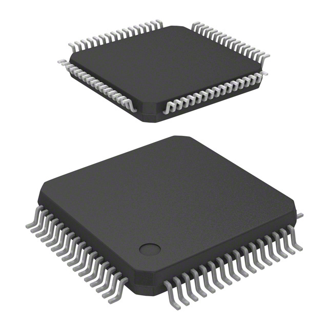
| Description: | IC MCU 16BIT 128KB FLASH 64LQFP |
| Package: | 64-LQFP |
| Quantity: | 5046 PCS |
| Lead Free Status / RoHS Status: | Lead free / RoHS Compliant |
| one to seven days | |
| Click buy button to purchase: | Buy |
CAD Models
There is no relevant information available for this part yet.
Lifecycle Status Indicator

S9S12G128F0CLH Lifecycle Status Indicator
Product Attributes
Manufacturer | Freescale Semiconductor - NXP |
Product Category | Embedded - Microcontrollers |
Series | HCS12 |
Mounting-Type | Surface Mount |
Brand | Freescale Semiconductor - NXP |
ADC Channels | 12 |
ADC Resolution | 10 bit |
Bit Size | 16 |
Core Size | 16-Bit |
Core Processor | 12V1 |
Core Architecture | HCS12 |
CPU Family | CPU12 |
Connectivity | LVD, POR, PWM, WDT |
Device Core | HCS12 |
Data Converters | A/D 12x10b |
Data Bus Width | 16 bit |
Data RAM Type | RAM |
Data ROM Size | 4 kB |
Data ROM Type | EEPROM |
Data Memory Size | 4 KB |
EEPROM Size | 4K x 8 |
Frequency | 25 MHz |
Family Name | HCS12 |
Interface Type | CAN/SCI/SPI |
Instruction Set Architecture | CISC |
JESD-30 Code | S-PQFP-G64 |
JESD-609 Code | e3 |
Lead Finish | Matte Tin |
Lead Shape | Gull-wing |
Memory Size | 128 kB |
Moisture Sensitivity Level | 3 |
Maximum Clock Rate | 25 MHz |
Maximum CPU Frequency | 25 MHz |
Maximum Expanded Memory Size | 256 KB |
Maximum Operating Supply Voltage | 5.5 V |
Minimum Operating Supply Voltage | 3.13 V |
Number of Timers | 1 |
Number of I/Os | 54 |
Number of Pins | 64 |
Number of Terminals | 64 |
Number of PWM Channels | 8 |
Number of ADC Channels | 12 |
On-Chip ADC | 12-chx10-bit |
Oscillator Type | Internal |
Operating Temperature-Min | -40.0 ℃ |
Operating Temperature-Max | 85.0 ℃ |
Pin Count | 64 |
PCB changed | 64 |
Packaging | Tray |
Peripherals | LVD, POR, PWM, WDT |
Power Supplies | 3.3/5 |
Product Type | 16-bit Microcontrollers - MCU |
Package Body Material | PLASTIC/EPOXY |
Package Code | QFP |
Package / Case | 64-LQFP |
Package Equivalence Code | QFP64,.47SQ,20 |
Package Shape | SQUARE |
Package Style | FLATPACK |
Programmability | Yes |
Program Memory Size | 128 KB |
Program Memory Type | FLASH |
RAM (bytes) | 8192.0 |
RAM Size | 8 KB |
ROM Programmability | FLASH |
ROM (words) | 131072 |
Speed | 25.0 MHz |
Sub Category | Microcontrollers |
Screening Level | Automotive |
Supplier Package | LQFP |
Supplier Device Package | 64-LQFP (10x10) |
Supply Voltage-Min | 3.13 V |
Supply Voltage-Max | 5.5 V |
Supply Current-Max | 23.0 mA |
Surface Mount | Yes |
Technology | CMOS |
Terminal Form | GULL WING |
Terminal Pitch | 0.5 mm |
Terminal Finish | Matte Tin (Sn) |
Terminal Position | QUAD |
Timers Channels | 8 |
Timers Resolution | 16 bit |
Temperature Grade | INDUSTRIAL |
Voltage - Supply (Vcc/Vdd) | 3.13 V ~ 5.5 V |
Height | 1.45 mm |
Length | 10.0 mm |
Width | 10.0 mm |
Watchdog | 1 |
Unit Weight | 0.012224 oz |
Overview
The MC9S12G-Family is an optimized, automotive, 16-bit microcontroller product line focused on low-cost, high-performance, and low pin-count. This family is intended to bridge between high-end 8-bit microcontrollers and high-performance 16-bit microcontrollers, such as the MC9S12XS-Family. The MC9S12G-Family is targeted at generic automotive applications requiring CAN or LIN/J2602 communication. Typical examples of these applications include body controllers, occupant detection, door modules, seat controllers, RKE receivers, smart actuators, lighting modules, and smart junction boxes.
The MC9S12G-Family uses many of the same features found on the MC9S12XS- and MC9S12P-Family, including error correction code (ECC) on flash memory, a fast analog-to-digital converter (ADC) and a frequency modulated phase locked loop (IPLL) that improves the EMC performance.
The MC9S12G-Family is optimized for lower program memory sizes down to 16k. In order to simplify customer use it features an EEPROM with a small 4 bytes erase sector size.
The MC9S12G-Family deliver all the advantages and efficiencies of a 16-bit MCU while retaining the low cost, power consumption, EMC, and code-size efficiency advantages currently enjoyed by users of Freescale’s existing 8-bit and 16-bit MCU families. Like the MC9S12XS-Family, the MC9S12G-Family run 16-bit wide accesses without wait states for all peripherals and memories. The MC9S12G-Family is available in 100-pin LQFP, 64-pin LQFP, 48-pin LQFP/QFN, 32-pin LQFP and 20-pin TSSOP package options and aims to maximize the amount of functionality especially for the lower pin count packages. In addition to the I/O ports available in each module, further I/O ports are available with interrupt capability allowing wake-up from stop or wait modes.
Features
On-chip modules available within the family include the following features:
• S12 CPU core
• Up to 240 Kbyte on-chip flash with ECC
• Up to 4 Kbyte EEPROM with ECC
• Up to 11 Kbyte on-chip SRAM
• Phase locked loop (IPLL) frequency multiplier with internal filter
• 4–16 MHz amplitude controlled Pierce oscillator
• 1 MHz internal RC oscillator
• Timer module (TIM) supporting up to eight channels that provide a range of 16-bit input capture, output compare, counter, and pulse accumulator functions
• Pulse width modulation (PWM) module with up to eight x 8-bit channels
• Up to 16-channel, 10 or 12-bit resolution successive approximation analog-to-digital converter (ADC)
• Up to two 8-bit digital-to-analog converters (DAC)
• Up to one 5V analog comparator (ACMP)
• Up to three serial peripheral interface (SPI) modules
• Up to three serial communication interface (SCI) modules supporting LIN communications
• Up to one multi-scalable controller area network (MSCAN) module (supporting CAN protocol 2.0A/B)
• On-chip voltage regulator (VREG) for regulation of input supply and all internal voltages
• Autonomous periodic interrupt (API)
• Precision fixed voltage reference for ADC conversions
• Optional reference voltage attenuator module to increase ADC accuracy
S12 CPU is a high-speed 16-bit processing unit:
• Full 16-bit data paths supports efficient arithmetic operation and high-speed math execution
• Includes many single-byte instructions. This allows much more efficient use of ROM space.
• Extensive set of indexed addressing capabilities, including:
— Using the stack pointer as an indexing register in all indexed operations
— Using the program counter as an indexing register in all but auto increment/decrement mode
— Accumulator offsets using A, B, or D accumulators
— Automatic index predecrement, preincrement, postdecrement, and postincrement (by –8 to +8)
On-chip flash memory on the MC9S12G-Family family features the following:
• Up to 240 Kbyte of program flash memory
— 32 data bits plus 7 syndrome ECC (error correction code) bits allow single bit error correction and double fault detection
— Erase sector size 512 bytes
— Automated program and erase algorithm
— User margin level setting for reads
— Protection scheme to prevent accidental program or erase
• Up to 4 Kbyte EEPROM
— 16 data bits plus 6 syndrome ECC (error correction code) bits allow single bit error correction and double fault detection
— Erase sector size 4 bytes
— Automated program and erase algorithm
— User margin level setting for reads
On-Chip SRAM
• Up to 11 Kbytes of general-purpose RAM
Port Integration Module (PIM)
• Data registers and data direction registers for ports A, B, C, D, E, T, S, M, P, J and AD when used as general-purpose I/O
• Control registers to enable/disable pull devices and select pullups/pulldowns on ports T, S, M, P, J and AD on per-pin basis
• Single control register to enable/disable pull devices on ports A, B, C, D and E, on per-port basis and on BKGD pin
• Control registers to enable/disable open-drain (wired-or) mode on ports S and M
• Interrupt flag register for pin interrupts on ports P, J and AD
• Control register to configure IRQ pin operation
• Routing register to support programmable signal redirection in 20 TSSOP only
• Routing register to support programmable signal redirection in 100 LQFP package only
• Package code register preset by factory related to package in use, writable once after reset. Also includes bit to reprogram routing of API_EXTCLK in all packages.
• Control register for free-running clock outputs
Main External Oscillator (XOSCLCP)
• Loop control Pierce oscillator using a 4 MHz to 16 MHz crystal
— Current gain control on amplitude output
— Signal with low harmonic distortion
— Low power
— Good noise immunity
— Eliminates need for external current limiting resistor
— Transconductance sized for optimum start-up margin for typical crystals
— Oscillator pins can be shared w/ GPIO functionality
Internal RC Oscillator (IRC)
• Trimmable internal reference clock.
— Frequency: 1 MHz
— Trimmed accuracy over –40˚C to +125˚C ambient temperature range:
±1.0% for temperature option C and V (see Table A-4)
±1.3% for temperature option M (see Table A-4)
Internal Phase-Locked Loop (IPLL)
• Phase-locked-loop clock frequency multiplier
— No external components required
— Reference divider and multiplier allow large variety of clock rates
— Automatic bandwidth control mode for low-jitter operation
— Automatic frequency lock detector
— Configurable option to spread spectrum for reduced EMC radiation (frequency modulation)
— Reference clock sources:
– External 4–16 MHz resonator/crystal (XOSCLCP)
– Internal 1 MHz RC oscillator (IRC)
System Integrity Support
• Power-on reset (POR)
• System reset generation
• Illegal address detection with reset
• Low-voltage detection with interrupt or reset
• Real time interrupt (RTI)
• Computer operating properly (COP) watchdog
— Configurable as window COP for enhanced failure detection
— Initialized out of reset using option bits located in flash memory
• Clock monitor supervising the correct function of the oscillator
Timer (TIM)
• Up to eight x 16-bit channels for input capture or output compare
• 16-bit free-running counter with 7-bit precision prescaler
• In case of eight channel timer Version an additional 16-bit pulse accumulator is available
Pulse Width Modulation Module (PWM)
• Up to eight channel x 8-bit or up to four channel x 16-bit pulse width modulator
— Programmable period and duty cycle per channel
— Center-aligned or left-aligned outputs
— Programmable clock select logic with a wide range of frequencies
Controller Area Network Module (MSCAN)
• 1 Mbit per second, CAN 2.0 A, B software compatible
— Standard and extended data frames
— 0–8 bytes data length
— Programmable bit rate up to 1 Mbps
• Five receive buffers with FIFO storage scheme
• Three transmit buffers with internal prioritization
• Flexible identifier acceptance filter programmable as:
— 2 x 32-bit
— 4 x 16-bit
— 8 x 8-bit
• Wakeup with integrated low pass filter option
• Loop back for self test
• Listen-only mode to monitor CAN bus
• Bus-off recovery by software intervention or automatically
• 16-bit time stamp of transmitted/received messages
Serial Communication Interface Module (SCI)
• Up to three SCI modules
• Full-duplex or single-wire operation
• Standard mark/space non-return-to-zero (NRZ) format
• Selectable IrDA 1.4 return-to-zero-inverted (RZI) format with programmable pulse widths
• 13-bit baud rate selection
• Programmable character length
• Programmable polarity for transmitter and receiver
• Active edge receive wakeup
• Break detect and transmit collision detect supporting LIN 1.3, 2.0, 2.1 and SAE J2602
Serial Peripheral Interface Module (SPI)
• Up to three SPI modules
• Configurable 8- or 16-bit data size
• Full-duplex or single-wire bidirectional
• Double-buffered transmit and receive
• Master or slave mode
• MSB-first or LSB-first shifting
• Serial clock phase and polarity options
Analog-to-Digital Converter Module (ADC)
Up to 16-channel, 10-bit/12-bit1 analog-to-digital converter
— 3 us conversion time
— 8-/101-bit resolution
— Left or right justified result data
— Wakeup from low power modes on analog comparison > or <= match
— Continuous conversion mode
— External triggers to initiate conversions via GPIO or peripheral outputs such as PWM or TIM
— Multiple channel scans
— Precision fixed voltage reference for ADC conversions
• Pins can also be used as digital I/O including wakeup capability
Reference Voltage Attenuator (RVA)
• Attenuation of ADC reference voltage with low long-term drift
Digital-to-Analog Converter Module (DAC)
• 1 digital-analog converter channel (per module) with:
— 8 bit resolution
— full and reduced output voltage range
— buffered or unbuffered analog output voltage usable
• operational amplifier stand alone usable
Analog Comparator (ACMP)
• Low offset, low long-term offset drift
• Selectable interrupt on rising, falling, or rising and falling edges of comparator output
• Option to output comparator signal on an external pin
• Option to trigger timer input capture events
On-Chip Voltage Regulator (VREG)
• Linear voltage regulator with bandgap reference
• Low-voltage detect (LVD) with low-voltage interrupt (LVI)
• Power-on reset (POR) circuit
• Low-voltage reset (LVR)
Background Debug (BDM)
• Non-intrusive memory access commands
• Supports in-circuit programming of on-chip nonvolatile memory
Debugger (DBG)
• Trace buffer with depth of 64 entries
• Three comparators (A, B and C)
— Access address comparisons with optional data comparisons
— Program counter comparisons
— Exact address or address range comparisons
• Two types of comparator matches
— Tagged This matches just before a specific instruction begins execution
— Force This is valid on the first instruction boundary after a match occurs
• Four trace modes
• Four stage state sequencer
The key performance parameters of S12G devices feature:
• Continuous Operating voltage of 3.15 V to 5.5 V
• Operating temperature (TA) of –40˚C to 125˚C
• Junction temperature (TJ) of up to 150˚C
• Bus frequency (fBus) of dc to 25 MHz
• Packaging:
— 100-pin LQFP, 0.5 mm pitch, 14 mm x 14 mm outline
— 64-pin LQFP, 0.5 mm pitch, 10 mm x 10 mm outline
— 48-pin LQFP, 0.5 mm pitch, 7 mm x 7 mm outline
— 48-pin QFN, 0.5 mm pitch, 7 mm x 7 mm outline
— 32-pin LQFP, 0.8 mm pitch, 7 mm x 7 mm outline
— 20 TSSOP, 0.65 mm pitch, 4.4 mm x 6.5 mm outline
— Known good die (KGD), unpackaged
Advantages and Disadvantages
There is no relevant information available for this part yet.
Applications
There is no relevant information available for this part yet.
Compliance
USHTS: | 8542310001 |
CAHTS: | 8542310000 |
CNHTS: | 8542319000 |
JPHTS: | 8542310324 |
KRHTS: | 8542311000 |
MXHTS: | 85423199 |
TARIC: | 8542319000 |
RoHS: | Compliance |
REACH SVHC: | No SVHC |
ECCN / UNSPSC
ECCN: | 3A991.A.2 |
HTSN: | 8542310001 |
SCHEDULE B: | 8542310000 |
Documents & Media
Datasheet | |
Environmental Information | |
PCN Design/Specification | |
Test/Quality Data | |
Product Manufacturer
NXP Semiconductors enables secure connections and infrastructure for a smarter world, advancing solutions that make lives easier, better and safer. As the world leader in secure connectivity solutions for embedded applications, NXP is driving innovation in the secure connected vehicle, end-to-end security & privacy and smart connected solutions markets. Built on more than 60 years of combined experience and expertise, the company has 45,000 employees in more than 35 countries.
Product Range
ARM ® PROCESSORS | ANALOG | POWER ARCHITECTURE ®PROCESSORS |
MEDIA AND AUDIO | RF | IDENTIFICATION & SECURITY |
Sensors | Wireless | Automotive Products |
Distributors
Distributors | Stock | Manufacturers | Descriptions |
Kynix | 5046 | Freescale Semiconductor - NXP | IC MCU 16BIT 128KB FLASH 64LQFP |
DigiKey | 775 | NXP USA Inc. | IC MCU 16BIT 128KB FLASH 64LQFP |
Mouser | 363 | NXP / Freescale | 16-bit Microcontrollers - MCU 16BIT 128K FLASH |
Alternative Models
There is no relevant information available for this part yet.
Popularity by Region

Market Price Analysis
There is no relevant information available for this part yet.
Pictures

S9S12G128F0CLH Images
 IC MCU 32BIT 256KB FLASH 100LQFP
 IC MCU 8BIT 1.75KB FLASH 8DFNS
 IC MCU 8BIT 8KB FLASH 8SOIC