| Manufacturer Part#: | MRF6S9130HR5 |
| Product Category: | IC chips |
| Manufacturer: | FREESCALE |
| Description: | NA |
| Package: | |
| Quantity: | 440 PCS |
| Lead Free Status / RoHS Status: | Lead free / RoHS Compliant |
| one to seven days | |
| Click buy button to purchase: | Buy |
DESCRIPTION
RF Power Field Effect Transistors
N-Channel Enhancement-Mode Lateral MOSFETs
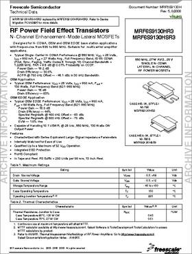
Designed for N - CDMA, GSM and GSM EDGE base station applications with frequencies from 865 to 960 MHz. Suitable for multicarrier amplifier applications.
• Typical Single-Carrier N-CDMA Performance @ 880 MHz: VDD = 28 Volts, IDQ = 950 mA, Pout = 27 Watts Avg., Full Frequency Band, IS-95 CDMA
(Pilot, Sync, Paging, Traffic Codes 8 Through 13) Channel Bandwidth = 1.2288 MHz. PAR = 9.8 dB @ 0.01% Probability on CCDF. Power Gain ó 19.2 dB,Drain Efficiency ó 30.5%,ACPR @ 750 kHz Offset ó -48.1 dBc in 30 kHz Bandwidth

APPLICATION
MRF6S9130HR3/HSR3 replaced by MRFE6S9130HR3/HSR3. Refer to Device Migration PCN12895 for more details.
Designed for N - CDMA, GSM and GSM EDGE base station applications with frequencies from to 960 MHz. Suitable for multicarrier amplifier applications. Typical Single - Carrier N - CDMA Performance @ 880 MHz: VDD = 28 Volts, IDQ = 950 mA, Pout = 27 Watts Avg., Full Frequency Band, - 95 CDMA (Pilot, Sync, Paging, Traffic Codes 8 Through 13) Channel Bandwidth = 1.2288 MHz. PAR @ 0.01% Probability on CCDF. Power Gain 19.2 dB Drain Efficiency 30.5% ACPR @ 750 kHz Offset - 48.1 dBc in 30 kHz Bandwidth GSM Application Typical GSM Performance: VDD = 28 Volts, IDQ = 950 mA, Pout = 130 Watts, Full Frequency Band - 960 MHz) Power Gain 18 dB Drain Efficiency 63% GSM EDGE Application Typical GSM EDGE Performance: VDD = 28 Volts, IDQ = 950 mA, Pout = 56 Watts Avg., Full Frequency Band - 960 MHz) Power Gain 18.5 dB Drain Efficiency 44% Spectral Regrowth @ 400 kHz Offset - 63 dBc Spectral Regrowth @ 600 kHz Offset - 75 dBc EVM 1.5% rms Capable of Handling 10:1 VSWR, @ 28 Vdc, 880 MHz, 130 Watts CW Output Power Features Characterized with Series Equivalent Large - Signal Impedance Parameters Internally Matched for Ease of Use Qualified to a Maximum of 32 VDD Operation Integrated ESD Protection RoHS Compliant In Tape and Reel. R3 Suffix = 250 Units per 56 mm, 13 inch Reel. Table 1. Maximum Ratings
Rating Drain- Source Voltage Gate- Source Voltage Storage Temperature Range Case Operating Temperature Operating Junction Temperature
Characteristic Thermal Resistance, Junction to Case Temperature W CW Case Temperature W CW Unit °C/W
1. Continuous use at maximum temperature will affect MTTF. 2. MTTF calculator available at http://www.freescale.com/rf. Select Software & Tools/Development Tools/Calculators to access MTTF calculators by product. 3. Refer to AN1955, Thermal Measurement Methodology of RF Power Amplifiers. Go to http://www.freescale.com/rf. Select Documentation/Application Notes - AN1955.
880 MHz, 27 W AVG., 28 V SINGLE N - CDMA LATERAL N - CHANNEL RF POWER MOSFETs
Test Methodology Human Body Model (per - A114) Machine Model (per - A115) Charge Device Model (per - C101) Class 1A (Minimum) A (Minimum) IV (Minimum)
Table 4. Electrical Characteristics (TC = 25°C unless otherwise noted)
Characteristic Off Characteristics Zero Gate Voltage Drain Leakage Current (VDS = 68 Vdc, VGS = 0 Vdc) Zero Gate Voltage Drain Leakage Current (VDS = 28 Vdc, VGS = 0 Vdc) IDSS IGSS 10 1 Adc Symbol Min Typ Max Unit
On Characteristics Gate Threshold Voltage (VDS = 10 Vdc, = 400 Adc) Gate Quiescent Voltage (VDD = 28 Vdc, = 950 mAdc, Measured in Functional Test) Drain- Source On - Voltage (VGS = 10 Vdc, = 2.74 Adc) Dynamic Characteristics (1) Output Capacitance (VDS = 28 Vdc ± 30 mV(rms)ac @ 1 MHz, VGS = 0 Vdc) Reverse Transfer Capacitance (VDS = 28 Vdc ± 30 mV(rms)ac @ 1 MHz, VGS = 0 Vdc) Coss Crss 1.6 pF VGS(th) VGS(Q) VDS(on) Vdc
Functional Tests (In Freescale Test Fixture, 50 ohm system) VDD = 28 Vdc, IDQ = 950 mA, Pout 27 W Avg. N - CDMA, = 880 MHz, Single - Carrier N - CDMA, 1.2288 MHz Channel Bandwidth Carrier. ACPR measured in 30 kHz Channel Bandwidth @ ±750 kHz Offset. PAR @ 0.01% Probability on CCDF Power Gain Drain Efficiency Adjacent Channel Power Ratio Input Return Loss Gps D ACPR IRL dB % dBc dB
Typical GSM EDGE Performances (In Freescale GSM EDGE Test Fixture, 50 ohm system) VDD = 28 Vdc, IDQ = 950 mA, Pout 56 W Avg., 921 MHz<Frequency<960 MHz Power Gain Drain Efficiency Error Vector Magnitude Spectral Regrowth at 400 kHz Offset Spectral Regrowth at 600 kHz Offset Gps D EVM dB % rms dBc
Typical CW Performances (In Freescale GSM Test Fixture, 50 ohm system) VDD = 28 Vdc, IDQ = 950 mA, Pout 921 MHz<Frequency<960 MHz Power Gain Drain Efficiency Input Return Loss Pout 1 dB Compression Point, = 940 MHz) 1. Part is internally matched on input. Gps D IRL dB W
Gate- Source Leakage Current (VGS = 5 Vdc, VDS = 0 Vdc)
Table 5. MRF6S9130HR3(SR3) Test Circuit Component Designations and Values
Part L1, L2 Description Ferrite Beads, Short 47 pF Chip Capacitors 8.2 pF Chip Capacitor 8.0 pF Variable Capacitors, Gigatrim 12 pF Chip Capacitors K pF Chip Capacitor 35 V Tantalum Chip Capacitors 10 pF Chip Capacitors 11 pF Chip Capacitor 4.5 pF Variable Capacitor, Gigatrim 50 V Chip Capacitor 63 V Electrolytic Capacitor 12.5 nH Inductors Part Number A04T- 5 Manufacturer Fair Rite ATC Johanson ATC Kemet ATC Johanson Kemet United Chemi - Con Coilcraft
x 0.080 Microstrip x 0.080 Microstrip x 0.220 Microstrip x 0.220 Microstrip x 0.220 Microstrip x 0.620 Taper
x 0.630 Microstrip x 0.630 Microstrip x 0.630 Microstrip x 0.630 Microstrip x 0.220 Microstrip x 0.220 Microstrip
FEATURES
• Characterized with Series Equivalent Large-Signal Impedance Parameters
• Internally Matched for Ease of Use
• Qualified Up to a Maximum of 32 VDD Operation
• Integrated ESD Protection
• RoHS Compliant
• In Tape and Reel. R3 Suffix = 250 Units per 56 mm, 13 inch Reel.
SPECIFICATION
| Manufacturer | FREESCALE |
| Product Category | IC Chips |
| Transistor Polarity | N-Channel |
| Vds - Drain-Source Breakdown Voltage | 68 V |
| Technology | Si |
| Minimum Operating Temperature | - 65 C |
| Maximum Operating Temperature | + 150 C |
| Mounting Style | SMD/SMT |
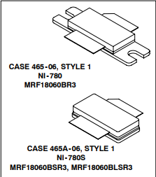
| Package / Case | NI-780 |
| Packaging | Reel |
| Configuration | Single |
| Height | 4.32 mm |
| Length | 34.16 mm |
| Width | 9.91 mm |
| Brand | NXP / Freescale |
| Channel Mode | Enhancement |
| Vgs - Gate-Source Voltage | - 0.5 V, 12 V |
| Unit Weight | 0.227150 oz |
RELEVANT POPULAR RESEARCHES
| PowerSO-10RF-Formed-4 RF MOSFET Transistors | 140 V RF MOSFET Transistors |
| N-Channel 100 mA RF MOSFET Transistors | 140 V RF MOSFET Transistors |
| Dual N-Channel RF MOSFET Transistors | 30 W Si SMD/SMT N-Channel RF MOSFET Transistors |
PICTURE


MRF6S9130HR5 image
 IC RS485/RS422 DATA INTRFC 24DIP
 low cost precision device designed for general purpose application
 CAP CER 0.022UF 50V X7R RADIAL