20
1. What is BJT Transistor
BJT transistors are three-terminal active devices made of two PN junctions, which are interacted with each other and fabricated on single crystals of semiconductor germanium or silicon to form a PNP (or NPN) structure. The N-type region in the middle is known as the Base (B), and the P-type regions on both sides are known as the Emitter (E) and the Collector (C), each of which has an lead called the B, the E and the C respectively, semiconductor electronic devices capable of amplifying, oscillating or switching.

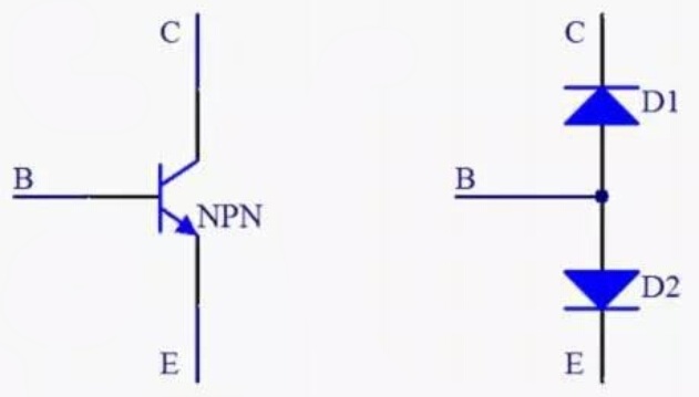
FIG.1 NPN transistor and its equivalent schematic diagram
Note: The above two diodes connected back to back is for illustration purpose only, otherwise how do we get the amplification function of the transistor? In other words, the transistor is not the same as the two diodes connected back to back!
2. What is the function of BJT transistor
(1) Transistor as a switch
Note: All transistors can be used as switches to control the opening and closing of a loop. The transistor used as a switch must be converted between the two states of cutoff and saturation, and not the active region.

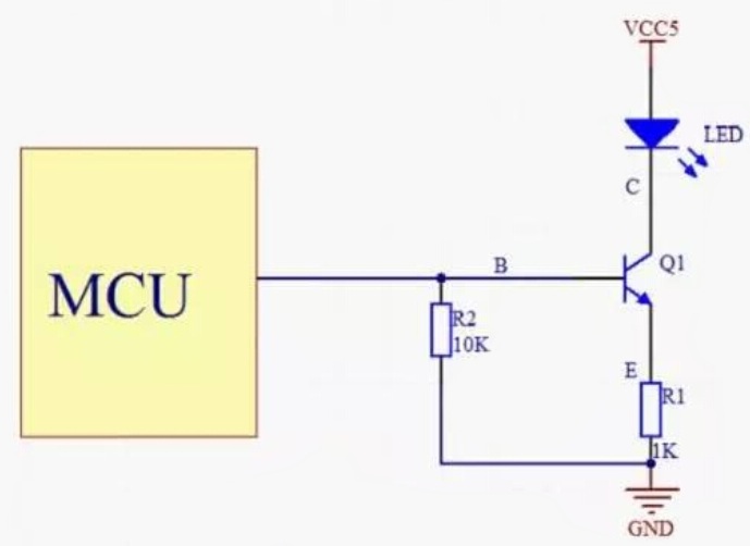
FIG.2 Simple transistor switching circuit
That is, when MCU outputs a high level, the transistor is in a saturation state, and at the same time the base-emitter junction & the base-collector junction are forward-biased, with a very low voltage between them, even lower than the conduction voltage of the PN junction (the conduction voltage of silicon tube is below 0.5V, and the standard value is 0.2V), therefore we can say that there is a short between C and E, an "on" state.
When MCU outputs a low level, the transistor is in a cutoff state, and at the same time the base-emitter junction & the base-collector junction are reverse-biased, with a very low current between them (almost no current can be measured on the silicon tube), therefore we can say that there is a break between C and E, an "off" state.
Note: R2 plays a role of pull-down, giving B a fixed level and leaving the transistor being off.
The characteristics of transistor Switching Circuit:
A. Switching speed is very fast, far faster than mechanical switches;
B. No mechanical contacts and no sparks;
C. Because of the high sensitivity, the switch has low requirements for control signals.
D. The voltage drop of the switch when it is turned on is larger than that of the mechanical switch, and the leakage current of the switch when it is turned off is larger than that of the mechanical switch.
E. Should not be used directly for high voltage, high current controls.
(2) Transistor as an amplifier
The amplifier circuit is to use the current control function of transistors or the voltage control function of FETs to amplify weak electric signals (or signals for short, the varying voltage, current or power) to the required value without distortion, and partially realize an energy transfer from the input signal of DC power supply to the output signal which varies regularly according to the input signal and has larger energy.
The amplifier circuit is actually an energy conversion device that uses a small amount of energy to control a larger energy conversion.
CIRCUIT COMPOSITION AND WORKING PRINCIPLE OF AMPLIFIER CIRCUIT:
A. There must be a DC power supply, and the power supply should be set to ensure that transistor or FET operates in a linear active region;
B. The arrangement of the components is to ensure the transmission of the signal, that is, to ensure that the signal can be input from the input end of the amplifier circuit, and output from the output end after amplified by the amplifier circuit;
C. When selecting component parameters, it is necessary to ensure that the signal can be amplified without distortion and meet the performance requirements of the amplifier circuit.
Note: In order to ensure that the transistor can normally amplify the signal, the base-emitter junction should be added with a forward voltage, and the base-collector junction should be added with a reverse voltage. Here, the basic principle of the transistor amplifier circuit is explained by taking the common-emitter amplifier circuit of the NPN transistor as an example. In the actual amplifying circuit, in addition to the common emitter mode, there are common collector configuration and common base configuration.

FIG.3 Bipolar Transistor Configurations
3. To give an example
(1) The common emitter amplifier circuit

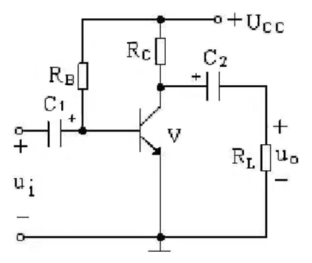
FIG.4 The Schematic Diagram of common emitter amplifier
(2) What are the roles of the components
A. The transistor V: Current amplification
B. DC POWER Supply: To ensure that the transistor works in an active region.
C. Load resistor RC: The current variations of the collector of the transistor are converted into voltage variations to achieve the voltage amplification.
D. Base bias resistor RB: Providing the operating point for the amplifier circuit.
E. Coupling capacitors C1 and C2: Blocking DC signals and allowing AC signals to pass.
(3) Working principles
A. The ui is added directly between the base and emitter of the transistor V, which causes the base current iB to increase and decrease accordingly.
B. The collector current iC of V will also change by the current amplification of V.
C. The variation of iC causes a voltage variation (uCE) between the collector and emitter of V.
D. The AC component uce in the uCE is smoothly transmitted to the load RL through C2, and becomes an AC voltage uo output, thereby realizing voltage amplification.
E. The AC component uce in the uCE is smoothly transmitted to the load RL through C2, and becomes an AC voltage uo to output, thereby realizing voltage amplification.
(4) DC analysis
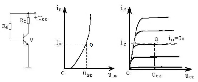
The objective of DC analysis is to obtain the quiescent (Q) point which usually determined by the DC path of amplifier circuit, as shown in the figure 5.

FIG.5 The DC path and the operating point of common emitter amplifier circuit
The invention of transistors revolutionized human civilization like no other technology. This video demonstrates working of a Bipolar Junction Transistor (BJT) with it's practical applications such as transistor as an amplifier and as a switch with help of animation. Along with transistor working of diode is also explained in the video. The video covers following topics - structure of Silicon atom, doping, N type doping, P type doping, working of Diode, working of NPN transistor and dual stage amplification.
Book Recommendation
Modular Series on Solid State Devices: Volume III: The Bipolar Junction Transistor(2nd Edition)
This book presents both a qualitative and quantitative description of the device. The second edition has been refined to improve pedagogical effectiveness.
by George W. Neudeck
Transistors For Toddlers
Perfect for all those toddlers looking to learn about electronics... or for a toddler whose parents will be entertained by a story about electronics while reading an alphabet book.
by David Signoff
You may also like:
Bipolar Junction Transistor|BJT Transistor Theory
MOSFET Gate Drive Circuit Guidelines - Hints & Tips
Simple Analog Circuit Examples for Electronic Engineers
Switched Mode Power Supply Design: SMPS Power Loss & Efficiency
Ordering & Quality
| Photo | Mfr. Part # | Company | Description | Package | Qty |
|
MC56F82743VLC | Company:NXP / Freescale | Remark:IC MCU 32BIT 64KB FLASH 32LQFP | Package:N/A |
MC56F82743VLC Datasheet |
In Stock:83 Inquiry |
Inquiry |
|
MPC8548EVTAUJC | Company:NXP / Freescale | Remark:IC MPU MPC85XX 1.333GHZ 783BGA | Package:783-BBGA, FCBGA |
MPC8548EVTAUJC Datasheet |
In Stock:842 Inquiry |
Inquiry |
|
K4S561632N-LC60 | Company:SAMSUNG | Remark:consumer memory | Package:TSOP |
K4S561632N-LC60 Datasheet |
In Stock:15960 Inquiry |
Inquiry |
|
SLB 9635 TT1.2 FW3.17 | Company:Infineon Technologies | Remark:IC SPECIALIZED | Package: |
SLB 9635 TT1.2 FW3.17 Datasheet |
In Stock:10854 Inquiry |
Inquiry |
|
FC4L110R050FER | Company:Ohmite | Remark:RES SMD 0.05 OHM 5W 4320 WIDE | Package:Wide 4320 (11050 Metric), 2043 |
FC4L110R050FER Datasheet |
In Stock:481 Inquiry |
Inquiry |
|
D2TO035CR0500FTE3 | Company:Vishay Sfernice | Remark:RES SMD 0.05 OHM 1% 35W TO263 | Package:TO-263-3, D²Pak (2 Leads + Tab), TO-263AB |
D2TO035CR0500FTE3 Datasheet |
In Stock:70 Inquiry |
Inquiry |
|
MAX14515EWA+T | Company:Maxim Integrated | Remark:IC LENS DVR SMALL LIQUID 8-WLP | Package:8-WFBGA, WLCSP |
MAX14515EWA+T Datasheet |
In Stock:9184 Inquiry |
Inquiry |
|
CAP017DG | Company:Power Integrations | Remark:IC CAP DISCHRG 1000V 2500NF 8SO | Package:8-SOIC (0.154", 3.90mm Width) |
CAP017DG Datasheet |
In Stock:7450 Inquiry |
Inquiry |
|
MC33910G5AC | Company:NXP | Remark:IC SYSTEM BASIS CHIP 32LQFP | Package:32-LQFP |
MC33910G5AC Datasheet |
In Stock:5153 Inquiry |
Inquiry |
|
MC68360ZQ25L | Company:Freescale Semiconductor - NXP | Remark:IC MPU M683XX 25MHZ 357BGA | Package:BGA |
MC68360ZQ25L Datasheet |
In Stock:811 Inquiry |
Inquiry |