10
The author perfected the content of this article on January 6th, 2020
Abstract
Semiconductor light-emitting diodes, abbreviated as LED, were developed from the 1960s and gradually became market-oriented. Its packaging technology is also continuously improved and developed. The development of LED from the earliest use of glass tube packaging to bracket epoxy packaging and surface mount packaging, making low-power LED widely used. Since the 1990s, due to breakthroughs in LED epitaxy and chip technology, quaternary AlGaInP and GaN-based LEDs have been introduced one after another, achieving full-color LED lighting, greatly enhanced brightness, and combining various colors and white light. The input power of the device has greatly improved. At present, single-chip 1W high-power LEDs have been industrialized and put to market, and Taiwan’s National Alliance has also developed 10W single-chip high-power LEDs. This makes the application area of ultra-high brightness LEDs continue to expand, first entering the market for special lighting, and advancing towards the general lighting market. As the input power of LED chips continues to increase, higher requirements are placed on the packaging technology of these power LED's. Power LED packaging technology should mainly meet the following two requirements: First, the package structure should have high light extraction efficiency, and second, the thermal resistance should be as low as possible to ensure the optoelectronic performance and reliability of the power LED. Therefore, this article will focus on the introduction and discussion of power LED packaging technology.
Catalog
Abstract | |
I Power LED Packaging Technology Status | |
II Foreign Power LED Packaging Technology | 1. Ordinary Power LED |
2. W-level Power LED | |
III Domestic Power LED Package Technology | |
IV The Key Packaging Technology of Power LED Industrialization | 1. Heat Dissipation |
2. Secondary Optical Design | |
3. Power LED White Light | |
4. Test Technology and Standards | |
5. Screening Technology and Reliability Assurance | |
6. Electrostatic Protection | |
V Market Trends of LED Packaging Technology | |
VI Book Recommendation | |
I Power LED Packaging Technology Status
Due to the wide application of power LEDs, the requirements for power LEDs vary from application to application. According to the power size, the current power type LED is divided into two kinds of general power LED and W-class power LED. LEDs with input power less than 1W (excluding tens of mW power LEDs) are normal power LEDs; LEDs with input power equal to or greater than 1W are W-level power LEDs. W-class power LEDs are commonly found in two forms, one is a single-chip W-class power LED, and the other is a multi-chip combined W-class power LED.
II Foreign Power LED Packaging Technology
1. Ordinary Power LED
According to the report, the LED of the "piranha" package structure was first introduced by HP in 1993 and was called "Super flux LED". In 1994, an improved "Snap LED" was introduced. Its appearance is shown in Figure 1. Their typical operating currents are 70mA and 150mA, respectively, and the input power is 0.1W and 0.3W, respectively.

Figure 1: Snap LED
Osram's "Power TOP LED" is a PLCC package structure with a metal frame. Its outline is shown in Figure 2. Later, some other companies introduced a variety of power LED package structure. One kind of PLCC-4 structural package form, its power is about 200~300mW, the thermal resistance of these structures is generally 75~125°C/W. In short, the power LED of these structures is several times higher than the LED input power of the original bracket type package, and the thermal resistance is several times lower.

Figure 2: Power TOP LED
2. W-level Power LED
The W-class power LED is the core part of the future lighting. Therefore, major companies in the world have invested a great deal of effort in the research and development of W-class power packaging technology, and have applied for various patents for the new structure and new technology. The single-chip W-class power LED was first introduced by Lumileds in 1998. The structure of the LED is shown in Figure 3. According to reports, the package structure is characterized by the use of thermoelectric separation in the form of a silicon carrier for flip chips. Welded on a heat sink, and using new structures and materials such as reflector cups, optical lenses, and flexible transparent adhesives, improved light extraction efficiency and improved heat dissipation characteristics. It can work stably and reliably at large current densities, and has a much lower thermal resistance than ordinary LEDs, typically 14~17°C/W, with existing 1W, 3W, and 5W products. The company also reported recently introduced Luxeon III LED products, which can be operated at higher driving currents due to improvements in packaging and chips, and can still maintain 70% lumens after operating at 700mA for 50,000 hours at 1A. 20,000 hours of work can maintain 50% lumens.
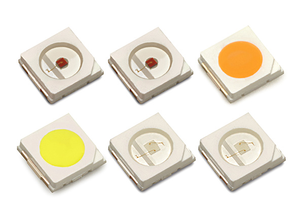
Figure 3: Luxeon LED
In 2003, Osram introduced a single-chip “Golden Dragon” series of LEDs. As shown in Figure 4, the structural characteristics of the LED are that the heat sink is in direct contact with the metal circuit board and has good heat dissipation performance, while the input power is good. 1W. China's Taiwanese company UEC (National Alliance) adopts Metal Bonding technology to encapsulate MB series high-power LED. Its characteristic is that Si is used instead of GaAs substrate, its heat dissipation is good, and the metal bonding layer is used as a light reflection layer to improve Light output. The current LED single chip area is: 0.3 & TImes; 0.3mm2, 1 & TImes; 1mm2 and 2.5 & TImes; 2.5mm2 chip, the input power of 0.3W, 1W and 10W, in which 2.5 & TImes; 2.5mm2 chip luminous flux up to 200lm , 0.3W and 1W products are on the market. The high-power LEDs of multi-chip combo packages have many structures and package types. Here are some typical structural package types:
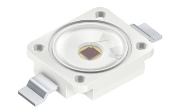
Figure 4: Golden Dragon LED
In 2001, UOE of the United States introduced a multi-chip packaged Norlux series of LEDs. The structure uses a hexagonal aluminum plate as the substrate. As shown in Figure 5, the aluminum layer is well-conducted, and the central luminous region can be assembled with 40 pieces. The chip, the package can be a single color or multi-color combination, can also be arranged according to the actual needs of the number of chips and gold wire welding, the package of high-power LED's luminous flux efficiency of 20lm / W, luminous flux of 100lm.

Figure 5: Norlux LED
Lanina Ceramics launched the high-power LED array using the company's proprietary Low Temperature Sintered Ceramic on Metal Substrate (LTCC-M) technology in 2003. There are two types of products: one is a 7-element LED array and the luminous flux is 840lm. The power is 21W. The other is a 134-yuan LED array with a luminous flux of 360lm and a power of 134W. Because the LTCC-M technology directly connects the LED chip to the sealed array configured package, the operating temperature can reach 250°C.
Panasonic introduced a high-power white LED with 64 chips combined in 2003. The luminous flux can reach 120lm. The substrate with excellent heat dissipation performance is packaged in an area of 2cm2, and its driving current can be reached to 8W, the temperature rise in this package is only 1.2°C per 1W input power.
Asian company launched in 2003 what is known as the world's brightest white LED, its luminous flux up to 600lm. When the output beam is 1000lm, the power consumption is 30W, the maximum input power is 50W, provides the white LED module display luminous efficiency up to 33lm/W. With regard to high-power LEDs with multi-chip combination, many companies constantly develop new products with new structure packaging according to the actual market demand, and their development speed is very fast.
III Domestic Power LED Package Technology
The domestic LED general product's post-process packaging capability should be very strong, and the variety of packaged products is relatively complete. According to preliminary estimates, there are more than 200 LED packaging factories in China and the packaging capacity exceeds 20 billion/year, and the packaging supporting capacity is also very strong. However, many packaging plants are private companies, and the current scale is small.
The packaging of domestic power-type LEDs began as early as the 1990s, and some powerful post-package companies began to develop and mass-produce them at the time, such as "piranhas" power LEDs. Domestic universities and research institutes rarely conduct research on high-power LED packaging technology. The 13th Institute of the Ministry of Information Industry conducts research work on power-type LED packaging technology and has achieved very good research results, specifically developing power LED products.
Domestic LED packaging companies (except foreign investment), such as Foshan Guoxing, Xiamen Hualian, and several other companies, have started developing R&D work on power LEDs early and achieved good results. Products such as "Piranha" and PLCC packages can be mass-produced, and single-chip, 1W class, high-power LED package samples have been developed. In addition, research and development of high-power LEDs with multi-chip or multi-device combinations are also available, and some samples can be provided for trial use. The research and development of high-power LED packaging technology, the country has not officially supported the investment, domestic research units rarely intervene, packaging companies invested in R & D efforts (manpower and financial resources) is still not enough, the formation of the domestic development of packaging technology is weak Compared with foreign countries, there is still a considerable gap in the technical level of its packaging.
IV The Key Packaging Technology of Power LED Industrialization
Semiconductor LEDs need to be used as lighting sources. The luminous flux of conventional products is far from that of general-purpose light sources such as incandescent lamps and fluorescent lamps. Therefore, in order to develop LEDs in the field of lighting, the key is to increase their luminous efficiency and luminous flux to the level of existing lighting sources. Although the epitaxial growth technology and multi-quantum well structure of MOCVD epitaxial materials are used for power LEDs, the external quantum efficiency needs to be further improved. However, the biggest obstacle to obtaining high luminous flux is still low light extraction efficiency of the chip. The existing power LED design adopts a flip-chip new structure to improve the light extraction efficiency of the chip, improve the thermal characteristics of the chip, and improve the photoelectric conversion efficiency of the device by increasing the chip area and increasing the operating current. Higher luminous flux. In addition to the chip, the packaging technology of the device also plays an important role. The key packaging technology processes are:
1. Heat Dissipation
The traditional indicator LED package structure is generally mounted on a small-sized reflector cup or a carrier table by using a conductive or non-conductive adhesive, and the internal and external connections of the device are completed by gold wire and encapsulated by epoxy resin. Its thermal resistance is as high as 250~300°C/W. If a new power chip adopts a traditional LED package, the junction temperature of the chip will rise rapidly and the carbonization of the epoxy will turn yellow due to poor heat dissipation, resulting in acceleration of the device. Decline until failure, even because the stress caused by the rapid thermal expansion causes an open circuit to fail. Therefore, for a power LED with a large operating current, a new package structure with low thermal resistance, good heat dissipation, and low stress is the key to the power LED device. The chip is bonded with a material with low resistivity and high thermal conductivity; a copper or aluminum heat sink is added to the lower part of the chip, and a semi-encapsulated structure is used to accelerate heat dissipation; even a secondary heat sink is designed to reduce the thermal resistance of the device. Inside the device, filled with highly flexible silicone rubber, in the silicone rubber temperature range (typically -40 °C ~ 200 °C), the colloid will not cause a sudden change in temperature and cause the device to open, it will not appear yellow phenomenon. The material of the part should also fully consider its thermal conductivity and heat dissipation characteristics in order to obtain good overall thermal characteristics.
2. Secondary Optical Design
In order to improve the light extraction efficiency of the device, an additional reflector cup and multiple optical lenses are designed.
3. Power LED White Light
There are three common methods for achieving white light:
(1) The blue chip is coated with a YAG phosphor, and the blue light of the chip excites the phosphor to emit yellow-green light with a typical value of 500 nm to 560 nm, and the yellow, green, and blue light synthesizes white light. The method is relatively simple to prepare, efficient and practical. The disadvantages are poor conformity of the glue, poor precipitation uniformity of the light emitting surface, poor color consistency, high color temperature, and poor color rendering.
(2) RGB Three primary colors, multiple chips or multiple devices emitting light to white light, or using blue + yellow-green complementary chips to generate white light. As long as the heat dissipation is effective, the white light produced by this method is more stable than the previous method, but the drive is more complex and the different light decay speeds of the different color chips have to be considered.
(3) Apply RGB phosphor on the UV chip, and use purple light to excite the phosphor to produce three primary colors of light to form white light. However, current UV chips and RGB phosphors have low efficiency, and epoxy resins are easily decomposed and aged under ultraviolet light irradiation. We currently use methods 1) and 2) for the mass production of white LED products, and have carried out prototype production of W-rated power LEDs. Accumulated a certain amount of experience and experience, we believe that to achieve industrialization of W-level power LED lighting products must also solve the following technical problems:
1)Powder coating control: LED chip + phosphor technology used in the coating method is usually the phosphor and glue mixed with a dispenser to apply it to the chip. In the process of operation, since the viscosity of the carrier rubber is a dynamic parameter, the specific gravity of the phosphor is greater than that of the carrier rubber and the dispenser is generated.
With the influence of factors such as accuracy, the control of the uniformity of the coating amount of the phosphor powder is difficult, resulting in non-uniform white light color.
2)Chip optoelectronic parameter coordination: the characteristics of semiconductor technology, determine the same material on the same wafer chip may exist between the optical parameters (such as wavelength, light intensity) and electrical (such as forward voltage) parameter differences. This is especially true for RGB trichromatic chips, which have a great influence on the white chromaticity parameters. This is one of the key technologies that must be addressed in industrialization.
According to the application requirements of the light color parameter control: different uses of the product, the white LED color coordinates, color temperature, color rendering, optical power (or light intensity) and the spatial distribution of light and other requirements are different. The control of the above parameters involves the coordination of various factors such as product structure, process methods, and materials. In industrialized production, it is very important to control the above factors and obtain products with good consistency and application requirements.
4. Test Technology and Standards
With the development of W-class power chip manufacturing technology and white LED process technology, LED products are gradually entering the (special) lighting market. The traditional LED product parameter detection standards and test methods for display or indication cannot meet the needs of lighting applications. Semiconductor equipment manufacturers at home and abroad have also launched their own test instruments. There are certain differences in the test principles, conditions, and standards for the use of different instruments, which increases the difficulty and complexity of test application and product performance comparison.
China Optoelectronics Optoelectronics Industry Association Photoelectron Devices Subcommittee Industry Association issued the “Light Emitting Diode Test Method (Trial)” in 2003 based on the needs of LED product development. The test method has increased the LED color parameter specification. However, the development of LED lighting industry, the establishment of LED lighting product standards is an important means of industry standardization.
5. Screening Technology and Reliability Assurance
Due to the limitation of the appearance of the luminaire, the assembly space of the lighting LED is sealed and limited. The sealed and limited space is not conducive to the heat dissipation of the LED, which means that the use environment of the lighting LED is inferior to the traditional display and instruction LED products. In addition, the lighting LED is driven by a large current, which imposes higher reliability requirements on it. In industrial production, appropriate heat aging, temperature cycling impact, and load aging process screening tests are developed for different product applications. It is necessary to eliminate early failure products and ensure product reliability.
6. Electrostatic Protection
The blue chip of the sapphire substrate has its positive and negative electrodes located on the chip with very small pitches. For InGaN/AlGaN/GaN double heterojunctions, the InGaN active mask layer is only a few tens of nanometers, and the electrostatic capacity is very small. Breakdown by static electricity causes the device to fail. Therefore, in the industrial production, the proper prevention of static electricity directly affects the product yield, reliability and economic benefits. Static electricity prevention techniques are as follows:
(1)Production and use places Protection from the transmission, stacking, etc. of the human body, Taiwan, land, space and products, such as anti-static clothing, gloves, wristbands, shoes, pads, boxes, ion fans, and testing instruments.
(2)ESD protection circuits are designed on the chip.
(3)LEDs are equipped with protective devices.
Illumitex LED Package Manufacturing Process
V Market Trends of LED Packaging Technology
As above , LED Package technology has an optimistic market prospect. In order to get high power,high brightness LED light sources,manufcacturers is now making efforts to produce high power LED with proper packages.t present, LED packages that can endure W scale power have been invented, such as Norlux Series high power LED package. It is a multi-chip assembly with a hexagon aluminum base board that functions as heat sink at the same time. Base board’s diameter amounts to 31.75mm. The emitting zone is located in its central part, with diameter of about (0.375×25.4)mm. Forty LED chips can be contained in one package. Generally, the future outlook for high-power-LED package is promising due to its high density chip assembly, high luminescence efficiency, low thermal resistance and high output power under large current flow. The thermal characteristics of power LED can directly influence its working temperature, luminescence efficiency, wavelength, life-span and other factors. Pay more attentions on the packaging design process,manufacturing technology of power LED chips is significant.
VI Book Recommendation
1. LED Packaging for Lighting Applications: Design, Manufacturing, and Testing
Since the first light-emitting diode (LED) was invented by Holonyak and Bevacqua in 1962, LEDs have made remarkable progress in the past few decades with the rapid development of epitaxy growth, chip design and manufacture, packaging structure, processes, and packaging materials. LEDs have superior characteristics such as high efficiency, small size, long life, low power consumption, and high reliability. The market for white LED is growing rapidly in various applications. It has been widely accepted that white LEDs will be the fourth illumination source to substitute the incandescent, fluorescent, and high-pressure sodium lamps. With the development of LED chip and packaging technologies, the efficiency of high power white LED will broaden the application markets of LEDs while changing the lighting concepts of our lives.
by Sheng Liu, Xiaobing Luo
2. Semiconductor Packaging: Materials Interaction and Reliability
The book focuses on an important step in semiconductor manufacturing―package assembly and testing. It covers the basics of material properties and explains how to determine which behaviors are important to package performance. The authors also discuss how the properties of packaging materials interact with each another and explore how to maximize the performance of these materials in regard to package integrity and reliability.
by Andrea Chen, Randy Hsiao-Yu Lo
You may also like:
The Sino-US comparison in Information Technology
Ordering & Quality
| Photo | Mfr. Part # | Company | Description | Package | Qty |
|
TMS320DM6433ZWTQ5 | Company:Texas Instruments | Remark:IC DGTL MEDIA PROCESSOR 361-BGA | Package:361-LFBGA |
TMS320DM6433ZWTQ5 Datasheet |
In Stock:485 Inquiry |
Inquiry |
|
SL811HST-AXC | Company:Cypress Semiconductor Corp | Remark:IC USB HOST/SLAVE CTRLR 48TQFP | Package:TQFP |
SL811HST-AXC Datasheet |
In Stock:15200 Inquiry |
Inquiry |
|
70V7599S166BCI8 | Company:IDT | Remark:SRAM 128K x 36 Synchronous Bank-Switchable Dual-Port SRAM | Package: |
70V7599S166BCI8 Datasheet |
In Stock:2 Inquiry |
Inquiry |
|
MCIMX6U7CVM08AC | Company:NXP / Freescale | Remark:IC MPU I.MX6DL 800MHZ 624MAPBGA | Package:624-LFBGA |
MCIMX6U7CVM08AC Datasheet |
In Stock:95 Inquiry |
Inquiry |
|
MC9S12C32CPBE25 | Company:NXP / Freescale | Remark:IC MCU 16BIT 32KB FLASH 52LQFP | Package:52-LQFP |
MC9S12C32CPBE25 Datasheet |
In Stock:951 Inquiry |
Inquiry |
|
MC908JL8MDWE | Company:NXP / Freescale | Remark:IC MCU 8BIT 8KB FLASH 28SOIC | Package:28-SOIC (0.295", 7.50mm Width) |
MC908JL8MDWE Datasheet |
In Stock:1023 Inquiry |
Inquiry |
|
DS1233DZ-15+T&R | Company:Maxim Integrated | Remark:IC 4.125V NO PBR 15% SOT223 | Package:TO-261-4, TO-261AA |
DS1233DZ-15+T&R Datasheet |
In Stock:3228 Inquiry |
Inquiry |
|
MCF52256AG80 | Company:NXP / Freescale | Remark:IC MCU 32BIT 256KB FLASH 144LQFP | Package:144-LQFP |
MCF52256AG80 Datasheet |
In Stock:2345 Inquiry |
Inquiry |
|
MR27T12800J | Company:OKI | Remark: | Package:TSSOP-48 |
MR27T12800J Datasheet |
In Stock:710 Inquiry |
Inquiry |
|
MC9S12C64CPBE | Company:NXP / Freescale | Remark:IC MCU 16BIT 64KB FLASH 52LQFP | Package:52-LQFP |
MC9S12C64CPBE Datasheet |
In Stock:2429 Inquiry |
Inquiry |